Intel's Haswell Architecture Analyzed: Building a New PC and a New Intel
by Anand Lal Shimpi on October 5, 2012 2:45 AM ESTTSX
Johan did a great job explaining Haswell's Transactional Synchronization eXtensions (TSX), so I won't go into as much depth here. The basic premise is simple, although the implementation is quite complex.
It's easy to demand well threaded applications from software vendors, but actually implementing code that scales well across unlimited threads isn't easy. Parallelizing truly independent tasks is the low hanging fruit, but it's the tasks that all access the same data structure that can create problems. With multiple cores accessing the same data structure, running independent of one another, there's the risk of two different cores writing to the same part of the same structure. Only one set of data can be right, but dealing with this concurrent access problem can get hairy.

The simplest way to deal with it is simply to lock the entire data structure as soon as one core starts accessing it and only allow that one core write access until it's done. Other cores are given access to the data structure, but serially, not in parallel to avoid any data integrity issues.
This is by far the easiest way to deal with the problem of multiple threads accessing the same data structure, however it also prevents any performance scaling across multiple threads/cores. As focused as Intel is on increasing single threaded performance, a lot of die area goes wasted if applications don't scale well with more cores.
Software developers can instead choose to implement more fine grained locking of data structures, however doing so obviously increases the complexity of their code.
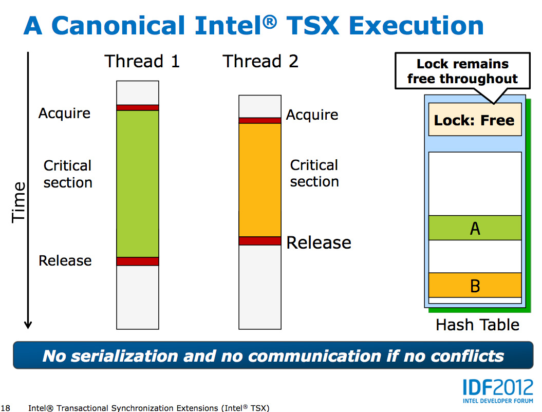
Haswell's TSX instructions allow the developer to shift much of the complexity of managing locks to the CPU. Using the new Hardware Lock Elision and its XAQUIRE/XRELEASE instructions, Haswell developers can mark a section of code for transactional execution. Haswell will then execute the code as if no hardware locks were in place and if it completes without issues the CPU will commit all writes to memory and enjoy the performance benefits. If two or more threads attempt to write to the same area in memory, the process is aborted and code re-executed traditionally with locks. The XAQUIRE/XRELEASE instructions decode to no-ops on earlier architectures so backwards compatibility isn't a problem.

Like most new instructions, it's going to take a while for Haswell's TSX to take off as we'll need to see significant adoption of Haswell platforms as well as developers embracing the new instructions. TSX does stand to show improvements in performance anywhere from client to server performance if implemented however, this is definitely one to watch for and be excited about.
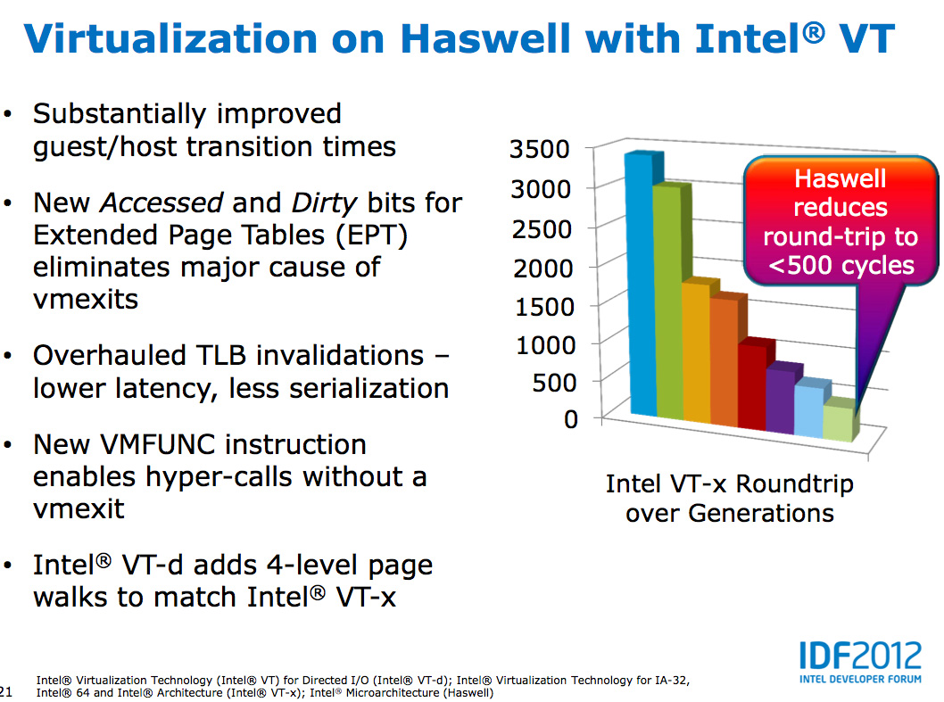
Haswell also continues improvements in virtualization performance, including big decreases to guest/host transition times.


245 Comments
View All Comments
kukreknecmi - Friday, October 5, 2012 - link
I hope i know it right. L3 on SB/IB doest used by GPU. L3 still servers as cache on system via memory controller. If GPU nneds to acess to memory, it sends request to memory controller. L3 is not directly accessable to GPU as a texture cache etc.On IB, they added a 512k cache which is seperated to half, 256k of it is used as texture system as backfeeding and other 256k half is used for other things.Article implies that L3 cache on IB is used as a texture buffer like on ordinary graphic cards. Only on Haswell L3 cache will be accessable and can be used as a some kind of GPU specific buffer.
Kevin G - Friday, October 5, 2012 - link
The confusing thing is that consumer Ivy Bridge parts have a L3 cache just for the GPU which is separate memory than the L3 cache that the CPU uses. The Ivy Bridge GPU's can use the CPU's L3 cache as the GPU's L4 cache to a degree.To confuse things further, the CPU side really has four levels of cache too. There is the small 1.5 KB micro-uop cache for instructions which comes before the 32 KB L1 instruction cache.
mayankleoboy1 - Friday, October 5, 2012 - link
From the article, its not very clear : Which platform (DT, Mobile, ultra mobile) will have the integrated voltage regulators/controllers ?Ryan Smith - Friday, October 5, 2012 - link
Ultra Mobile.Anand Lal Shimpi - Friday, October 5, 2012 - link
It's not clear how much of the VR circuitry gets integrated into Haswell or necessarily which parts will have it and which ones won't. Ultra mobile is a shoe in, but I've even heard of desktop parts getting it as well. We'll have to wait and see.DanNeely - Friday, October 5, 2012 - link
Rats. Reading the article I was hoping that Intel had decided to only bake the VRMs into their ultra-mobile parts. Better VRMs are an important factor in high end OCing; with desktop boards not cramped for space I really hope Intel keeps them off the package.Peanutsrevenge - Friday, October 5, 2012 - link
Seconded.However, I wonder whether the VRMs on high end mobos will still be an option, where the on package VRMs will simply extend the capabilities?
But given Intels recent distaste for overclocking, it wouldn't suprise me if we'll soon see CPUs completely locked from overclocking completely or only on E series, high profit chips.
Homeles - Saturday, October 6, 2012 - link
"However, I wonder whether the VRMs on high end mobos will still be an option, where the on package VRMs will simply extend the capabilities?"Bingo.
Homeles - Saturday, October 6, 2012 - link
Low end motherboards won't need them. High end overclocking boards will have them in addition to the ones on package.tuxRoller - Friday, October 5, 2012 - link
Using lvds reclocking you can reduce idle screen induced wakeups to 30 (ditto for the memory controller if the cpu supports self refresh for the sram ).eDP may allow even less.