NVIDIA GeForce GTX 670 Review Feat. EVGA: Bringing GK104 Down To $400
by Ryan Smith on May 10, 2012 9:00 AM ESTMeet The GeForce GTX 670
Because of the relatively low power consumption of GK104 relative to past high-end NVIDIA GPUs, NVIDIA has developed a penchant for small cards. While the GTX 680 was a rather standard 10” long, NVIDIA also managed to cram the GTX 690 into the same amount of space. Meanwhile the GTX 670 takes this to a whole new level.
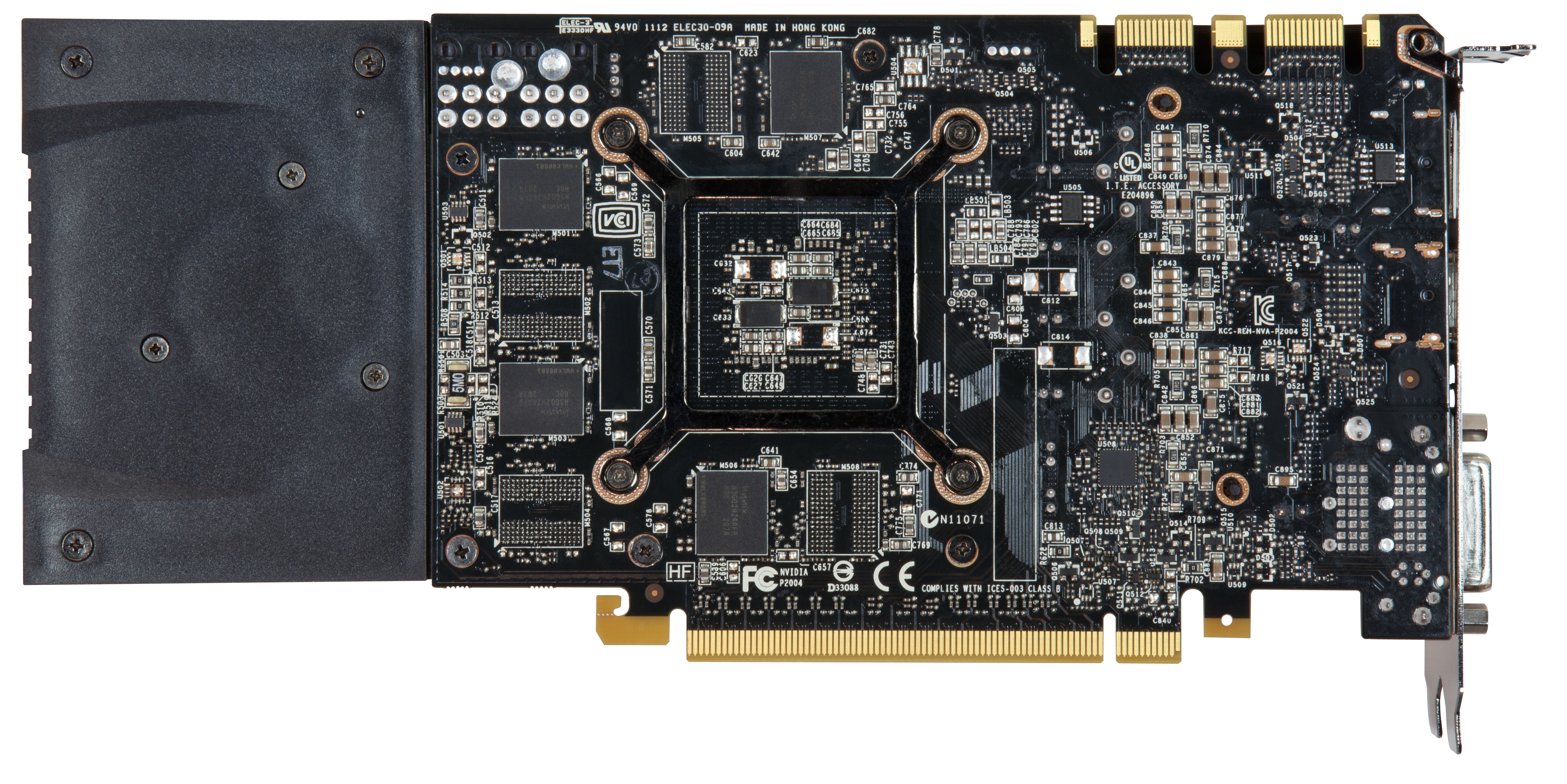
We’ll start at the back as this is really where NVIDIA’s fascination with small size makes itself apparent. The complete card is 9.5” long, however the actual PCB is far shorter at only 6.75” long, 3.25” shorter than the GTX 680’s PCB. In fact it would be fair to say that rather than strapping a cooler onto a card, NVIDIA strapped a card onto a cooler. NVIDIA has certainly done short PCBs before – such as with one of the latest GTX 560 Ti designs – but never on a GTX x70 part before. But given the similarities between GK104 and GF114, this isn’t wholly surprising, if not to be expected.
In any case this odd pairing of a small PCB with a large cooler is no accident. With a TDP of only 170W NVIDIA doesn’t necessarily need a huge PCB, but because they wanted a blower for a cooler they needed a large cooler. The positioning of the GPU and various electronic components meant that the only place to put a blower fan was off of the PCB entirely, as the GK104 GPU is already fairly close to the rear of the card. Meanwhile the choice of a blower seems largely driven by the fact that this is an x70 card – NVIDIA did an excellent job with the GTX 560 Ti’s open air cooler, which was designed for the same 170W TDP, so the choice is effectively arbitrary from a technical standpoint (there’s no reason to believe $400 customers are any less likely to have a well-ventilated case than $250 buyers). Accordingly, it will be NVIDIA’s partners that will be stepping in with open air coolers of their own designs.
Starting as always at the top, as we previously mentioned the reference GTX 670 is outfitted with a 9.5” long fully shrouded blower. NVIDIA tells us that the GTX 670 uses the same fan as the GTX 680, and while they’re nearly identical in design, based on our noise tests they’re likely not identical. On that note unlike the GTX 680 the fan is no longer placed high to line up with the exhaust vent, so the GTX 670 is a bit more symmetrical in design than the GTX 680 was.
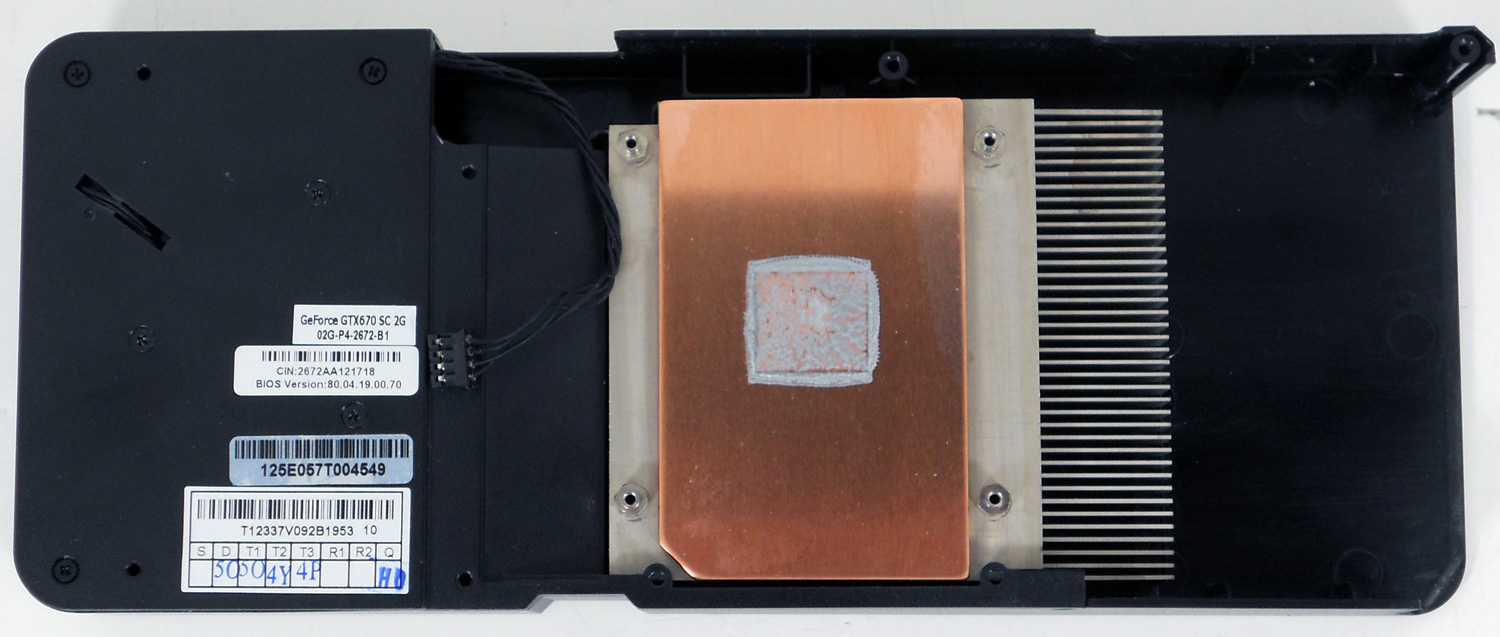
Note: We dissaembled the virtually identical EVGA card here instead
Lifting the cooler we can see that NVIDIA has gone with a fairly simple design here. The fan vents into a block-style aluminum heatsink with a copper baseplate, providing cooling for the GPU. Elsewhere we’ll see a moderately sized aluminum heatsink clamped down on top of the VRMs towards the front of the card. There is no cooling provided for the GDDR5 RAM.
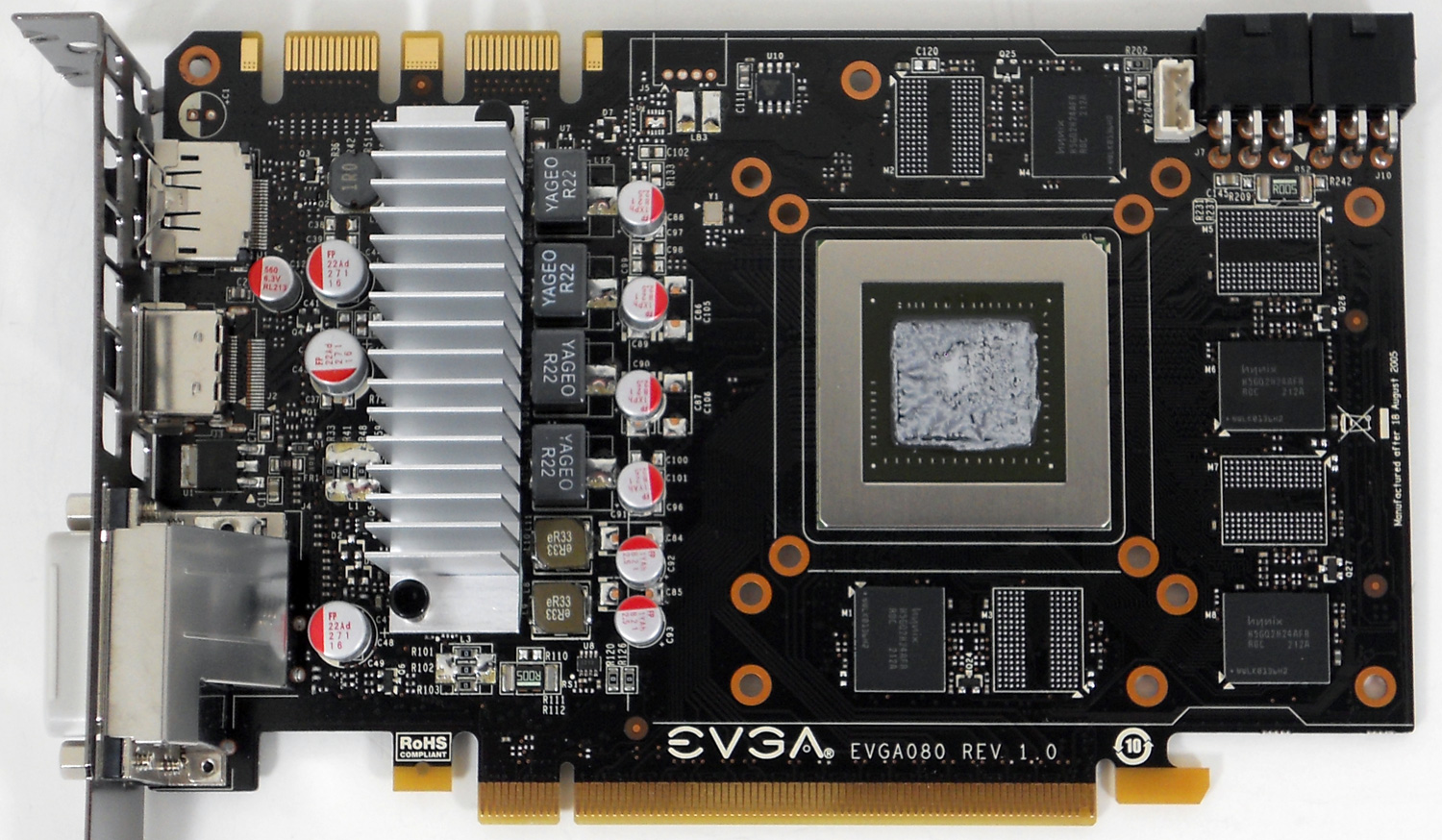
Note: We dissaembled the virtually identical EVGA card here instead
As for the PCB, as we mentioned previously due to the lower TDP of the GTX 670 NVIDIA has been able to save some space. The VRM circuitry has been moved to the front of the card, leaving the GPU and the RAM towards the rear and allowing NVIDIA to simply omit a fair bit of PCB space. Of course with such small VRM circuitry the reference GTX 670 isn’t built for heavy overclocking – like the other GTX 600 cards NVIDIA isn’t even allowing overvolting on reference GTX 670 PCBs – so it will be up to partners with custom PCBs to enable that kind of functionality. Curiously only 4 of the 8 Hynix R0C GDDR5 RAM chips are on the front side of the PCB; the other 4 are on the rear. We typically only see rear-mounted RAM in cards with 16/24 chips, as 8/12 will easily fit on the same side.


Elsewhere at the top of the card we’ll find the PCIe power sockets and SLI connectors. Since NVIDIA isn’t scrambling to save space like they were with the GTX 680, the GTX 670’s PCIe power sockets are laid out in a traditional side-by-side manner. As for the SLI connectors, since this is a high-end GeForce card NVIDIA provides 2 connectors, allowing for the card to be used in 3-way SLI.
Finally at the front of the card NVIDIA is using the same I/O port configuration and bracket that we first saw with the GTX 680. This means 1 DL-DVI-D port, 1 DL-DVI-I port, 1 full size HDMI 1.4 port, and 1 full size DisplayPort 1.2. This also means the GTX 670 follows the same rules as the GTX 680 when it comes to being able to idle with multiple monitors.


414 Comments
View All Comments
CeriseCogburn - Sunday, May 13, 2012 - link
This is your false claim about obviously. It's your and Charlie D's semi-accurate hit piece opinion and nothing else.dagamer34 - Thursday, May 10, 2012 - link
Products actually have to be consistently available for significant price drops like what you want to happen. Right now, if you need a high end card TODAY, waiting around for a GTX 680 isn't really an option, you'll have to go for the 7970 and AMD knows that.CeriseCogburn - Thursday, May 10, 2012 - link
Nope, 670 is all over the egg. Sorry you're late with that crap, and it's USA only BTW concerning 680 - the rest of the non obama world isn't suffering and can you really blame the asain(China/ commie cap government) manufacturers ?anubis44 - Friday, May 11, 2012 - link
"In the end they can't keep GK104 in stock anywhere and they still manage to beat AMD convincingly in both price and performance."You mean nvidia can't seem to make any. According to this article, nvidia has only been able to make a fraction of the GK104s that AMD has made Tahitis:
http://semiaccurate.com/2012/05/08/nvidias-five-ne...
That's what happens when you don't understand the manufacturing process you're moving to. You design a chip that's so ambitious, the failure rate is spectacular. AMD (and ATI before) on the other hand are much more familiar with the limits of successive process technology at TSMC, hence they are getting higher yields per wafer despite having a slightly larger die size, even without neutering their GPGPU compute circuitry like nvidia did.
eddman - Friday, May 11, 2012 - link
I wouldn't put too much weight in charlie's opinionated so called articles.CeriseCogburn - Friday, May 11, 2012 - link
If you read them on nVidia, and it is painful to see the twisted incoherent lies and completely contradictory links that disprove his stated reason for posting them or simply do not contain what he claimed they do, any bit of weight is too much weight at all.It's an amd fanboy firestarter flamer site, charlie's biggest purchase is red tipped matches and gasoline in a red can.
chizow - Sunday, May 13, 2012 - link
Can't agree with this for a lot of reasons. Maybe in the past with the huge GPU dies, but GK104 is *SMALLER* than Tahiti so there's really nothing ambitious about it.For capacities, Nvidia and TSMC have very close relationships and we know for a fact Nvidia is selling 2 GPUs for every 1 of AMDs, so Nvidia has an advantage there in terms of orders placed as well.
There's no reason to believe Nvidia is at any process disadvantage relative to AMD on 28nm, if anything everyone is supply constrained as other players try to move in (like Apple).
The fact there's plenty of GTX 670s still available after 3 days after launch with EXTREMELY favorable reviews tells me supply is excellent, and that Nvidia is only supply constrained on the high-end with perfect ASICs splitting good die between GTX 680 and 690.
chizow - Thursday, May 10, 2012 - link
Per usual Ryan, very relevant observations and interesting insight in regard to the changes Nvidia has made.I think I would take some of your first page insights a bit further:
1) GTX 680 is probably already heavily "overclocked" and binned to achieve a SKU Nvidia may not have planned originally, in order to beat the 7970 with a mid-range ASIC.
2) We will probably see an even more heavily harvested GK104 chip soon, given how little GTX 670 cuts from GTX 680 (just 1 SMX), but Nvidia can't cut too much without significantly impacting performance.
3) Pricing as you've laid out nicely, is probably $50-$100 too high across the board for all of these 28nm parts somewhere in the +20-25% premium range based on relative performance and historical pricing.
There's quite a few minor grammar errors throughout your article, nothing a quick proofread won't correct, but the content is excellent as usual.
Iketh - Thursday, May 10, 2012 - link
will you take the words "historical pricing" and remove them from your vocabulary? PLEASE?chizow - Thursday, May 10, 2012 - link
Its obvious the term is completely foreign to many here, including yourself, so until its well understood what it means and why its important and relevant to the discussion, I'll continue to use it."Those who do not learn from their mistakes are doomed to repeat them".
You're not even in a position to learn from your mistakes when you don't even understand the importance of "historical pricing".