NVIDIA GeForce GTX 680 Review: Retaking The Performance Crown
by Ryan Smith on March 22, 2012 9:00 AM ESTThe Kepler Architecture: Efficiency & Scheduling
So far we’ve covered how NVIDIA has improved upon Fermi for; now let’s talk about why.
Mentioned quickly in our introduction, NVIDIA’s big push with Kepler is efficiency. Of course Kepler needs to be faster (it always needs to be faster), but at the same time the market is making a gradual shift towards higher efficiency products. On the desktop side of matters GPUs have more or less reached their limits as far as total power consumption goes, while in the mobile space products such as Ultrabooks demand GPUs that can match the low power consumption and heat dissipation levels these devices were built around. And while strictly speaking NVIDIA’s GPUs haven’t been inefficient, AMD has held an edge on performance per mm2 for quite some time, so there’s clear room for improvement.
In keeping with that ideal, for Kepler NVIDIA has chosen to focus on ways they can improve Fermi’s efficiency. As NVIDIA's VP of GPU Engineering, Jonah Alben puts it, “[we’ve] already built it, now let's build it better.”
There are numerous small changes in Kepler that reflect that goal, but of course the biggest change there was the removal of the shader clock in favor of wider functional units in order to execute a whole warp over a single clock cycle. The rationale for which is actually rather straightforward: a shader clock made sense when clockspeeds were low and die space was at a premium, but now with increasingly small fabrication processes this has flipped. As we have become familiar with in the CPU space over the last decade, higher clockspeeds become increasingly expensive until you reach a point where they’re too expensive – a point where just distributing that clock takes a fair bit of power on its own, not to mention the difficulty and expense of building functional units that will operate at those speeds.
With Kepler the cost of having a shader clock has finally become too much, leading NVIDIA to make the shift to a single clock. By NVIDIA’s own numbers, Kepler’s design shift saves power even if NVIDIA has to operate functional units that are twice as large. 2 Kepler CUDA cores consume 90% of the power of a single Fermi CUDA core, while the reduction in power consumption for the clock itself is far more dramatic, with clock power consumption having been reduced by 50%.

Of course as NVIDIA’s own slide clearly points out, this is a true tradeoff. NVIDIA gains on power efficiency, but they lose on area efficiency as 2 Kepler CUDA cores take up more space than a single Fermi CUDA core even though the individual Kepler CUDA cores are smaller. So how did NVIDIA pay for their new die size penalty?
Obviously 28nm plays a significant part of that, but even then the reduction in feature size from moving to TSMC’s 28nm process is less than 50%; this isn’t enough to pack 1536 CUDA cores into less space than what previously held 384. As it turns out not only did NVIDIA need to work on power efficiency to make Kepler work, but they needed to work on area efficiency. There are a few small design choices that save space, such as using 8 SMXes instead of 16 smaller SMXes, but along with dropping the shader clock NVIDIA made one other change to improve both power and area efficiency: scheduling.
GF114, owing to its heritage as a compute GPU, had a rather complex scheduler. Fermi GPUs not only did basic scheduling in hardware such as register scoreboarding (keeping track of warps waiting on memory accesses and other long latency operations) and choosing the next warp from the pool to execute, but Fermi was also responsible for scheduling instructions within the warps themselves. While hardware scheduling of this nature is not difficult, it is relatively expensive on both a power and area efficiency basis as it requires implementing a complex hardware block to do dependency checking and prevent other types of data hazards. And since GK104 was to have 32 of these complex hardware schedulers, the scheduling system was reevaluated based on area and power efficiency, and eventually stripped down.
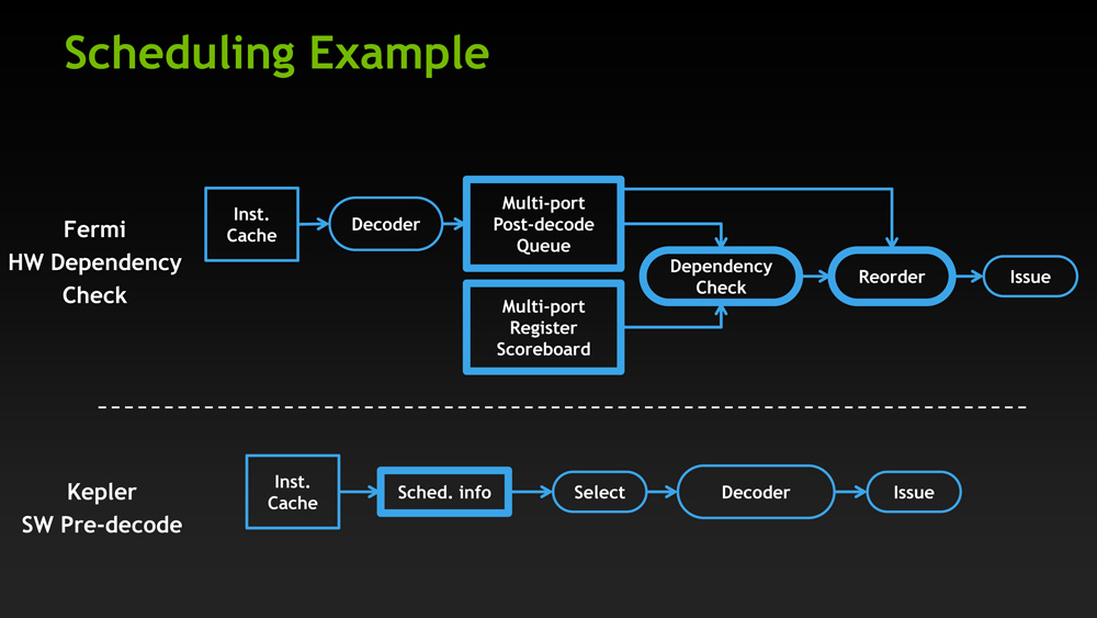
The end result is an interesting one, if only because by conventional standards it’s going in reverse. With GK104 NVIDIA is going back to static scheduling. Traditionally, processors have started with static scheduling and then moved to hardware scheduling as both software and hardware complexity has increased. Hardware instruction scheduling allows the processor to schedule instructions in the most efficient manner in real time as conditions permit, as opposed to strictly following the order of the code itself regardless of the code’s efficiency. This in turn improves the performance of the processor.
However based on their own internal research and simulations, in their search for efficiency NVIDIA found that hardware scheduling was consuming a fair bit of power and area for few benefits. In particular, since Kepler’s math pipeline has a fixed latency, hardware scheduling of the instruction inside of a warp was redundant since the compiler already knew the latency of each math instruction it issued. So NVIDIA has replaced Fermi’s complex scheduler with a far simpler scheduler that still uses scoreboarding and other methods for inter-warp scheduling, but moves the scheduling of instructions in a warp into NVIDIA’s compiler. In essence it’s a return to static scheduling.
Ultimately it remains to be seen just what the impact of this move will be. Hardware scheduling makes all the sense in the world for complex compute applications, which is a big reason why Fermi had hardware scheduling in the first place, and for that matter why AMD moved to hardware scheduling with GCN. At the same time however when it comes to graphics workloads even complex shader programs are simple relative to complex compute applications, so it’s not at all clear that this will have a significant impact on graphics performance, and indeed if it did have a significant impact on graphics performance we can’t imagine NVIDIA would go this way.
What is clear at this time though is that NVIDIA is pitching GTX 680 specifically for consumer graphics while downplaying compute, which says a lot right there. Given their call for efficiency and how some of Fermi’s compute capabilities were already stripped for GF114, this does read like an attempt to further strip compute capabilities from their consumer GPUs in order to boost efficiency. Amusingly, whereas AMD seems to have moved closer to Fermi with GCN by adding compute performance, NVIDIA seems to have moved closer to Cayman with Kepler by taking it away.
With that said, in discussing Kepler with NVIDIA’s Jonah Alben, one thing that was made clear is that NVIDIA does consider this the better way to go. They’re pleased with the performance and efficiency they’re getting out of software scheduling, going so far to say that had they known what they know now about software versus hardware scheduling, they would have done Fermi differently. But whether this only applies to consumer GPUs or if it will apply to Big Kepler too remains to be seen.


404 Comments
View All Comments
chizow - Thursday, March 22, 2012 - link
Nvidia let AMD off the hook by productizing a mid-range GK104 ASIC as their flagship SKU and pricing it at $500.Its a great part no doubt and beats AMD in every metric, but as the article stated, its still going to be the smallest increase in price:performance that we've seen since 9800GTX.
Overall 28nm has been a huge disappointment so far in terms of performance increase over previous generations at the same price points, I guess we will have to wait for 28nm BigK to get that true high-end increase you'd expect from a smaller process node and new GPU arch.
B-Unit1701 - Thursday, March 22, 2012 - link
'Off the hook'? LMAO they released what they had. They are already months late, the only other option would have been to just not release a card this generation, would THAT have made you happier?chizow - Thursday, March 22, 2012 - link
No, what would have made me happier from both Nvidia and AMD would be to follow their own historical price:performance metrics.Instead, we have AMD first trying to pass an overall unimpressive Tahiti part as a high-end flagship at $550+ followed by Nvidia following suit by pricing their mid-range ASIC as a $500 part.
28nm has been a big disappointment so far, as we have the smallest increase in price:performance in any generation or process shrink since the 9800GTX.
CeriseCogburn - Thursday, March 22, 2012 - link
With AMD GF foundry failures TSMC is stoked to the gills. We're not going to get the prices you want for performance for another 6 months or so when production is freed up with TSMC's ongoing 2B expansion.You ought to include real inflation as well which is as we all know far higher than the socialist government figures that are suppressed so their automatic payout increases are lessened.
Be disappointed, a valid point, there are extenuating factors.
xrror - Thursday, March 22, 2012 - link
exactly. I completely understand why Nvidia is charging $500 for their mid-range part, but it still sucks.AMD also... I get why the 6000 series was gimped (it was originally supposed to be 32nm, and that fell through) but 7000 series... maybe that can be explained by moving to a new arch with GCN.
Regardless... disappointing. Well actually it's dissapointing that you must pay $500+ to get a card that /might/ give you a fresh gaming experience over the $350 card you bought last generation.
Unless AMD can pull a 8000 gen card out of their arse with drivers that work (i'm not optimistic) then you can bet if/when "full Kepler" comes out it will be $800+
CeriseCogburn - Friday, March 23, 2012 - link
Charlie D with his $299 leak, the only source, has made everyone think the 1core top card in the world was going to be released $150 cheaper than the current top 1core card in the world.He must still be laughing hard at semi-accurate.
chizow - Friday, March 23, 2012 - link
It wasn't Charlie's leak, it was the combined evidence of ~300mm^2 size, transistor count, mid-range specs, ASIC designation, and leaked GTX 670Ti pics also leading people to the conclusion this part was originally meant to be priced in that $250-$350 range.Obviously GK104 performed better than expected, coupled with Tahiti being weaker than expected, resulting in what we see today: an exceptionally performing mid-range ASIC being SKU'd as an overpriced flagship part at premium pricing.
CeriseCogburn - Tuesday, March 27, 2012 - link
Sorry I don't buy any of it. It's a "new architecture", if we take Charlie's leak, everything fits but the price, and every price has been $499 going on 4X in a row at least.chizow - Friday, March 23, 2012 - link
I agree, but honestly I don't even think AMD can compete at this point. Nvidia has beaten AMD at its own game soundly (small die, power efficient strategy, and done it with their 2nd best ASIC.Now they're free to make the slightly faster, power-hungry GPGPU monster GPU with as much TDP as they like without having to hear about it being worst than AMD's tree-hugging specs.
Sabresiberian - Friday, March 23, 2012 - link
Nvidia releasing their new architecture a few months after AMD released theirs does not make them late. Nvidia's schedule hasn't been the same as AMD's for several years now.And, what's AMD's answer to Big Kepler going to be? They lost today to Nvidia's mid-line chip, they will lose big time when Big Kepler comes out. By the time they catch up, Maxwell will be breathing down their necks.
;)