NVIDIA's GeForce GTX 580: Fermi Refined
by Ryan Smith on November 9, 2010 9:00 AM ESTMeet the GTX 580
Since we’ve already discussed the cooling, let’s dive right in to the rest of the GTX 580, shall we?
Launching today will be a single GTX 580 design, the reference design. Talking to our contacts, semi-custom designs (designs using the reference PCB with a different cooler) are due in the next few weeks assuming everything goes to plan and of course there’s ample supply. And while we’re on that note, NVIDIA let us know that with their focus on cooling on the GTX 580 they aren’t going to be letting custom GTX 580 designs go out without a more thorough inspection. The acoustic performance of the reference GTX 580 is going to be the bare minimum to get a design approved – if it can’t beat the reference design, NVIDIA won’t allow it. We consider this a matter of brand protection for the company, as a bad/loud GeForce is still a GeForce all the same.
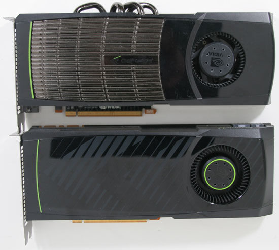
Top: GTX 480. Bottom: GTX580
With the reference design the resulting card is very close to being a GTX 285/480 hybrid. In terms of overall design it ends up looking very similar to the GTX 285. At 10.5” long it’s the same length as the GTX 480 or a smidge longer than the GTX 285, and should fit in to any cases those cards could work in. Power connectivity is the same as the GTX 480, with 6pin and 8pin PCIe sockets being located at the top of the card, providing easy access to the sockets. At 244W TDP the card draws too much for 6+6, but you can count on an eventual GTX 570 to fill that niche. Meanwhile NVIDIA has kept the 480’s detachable shroud lid, meaning you can remove the cover of the shroud without disturbing the rest of the card; it’s worth noting that it’s secured with screws rather than laches this time however.
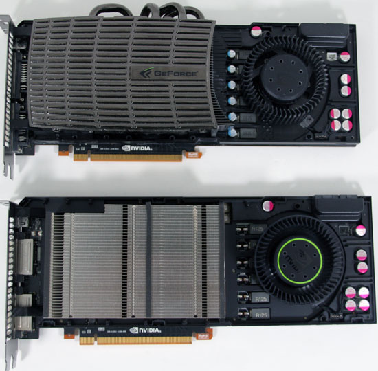
Heatsinks Exposed! Top: GTX 480. Bottom: GTX 580
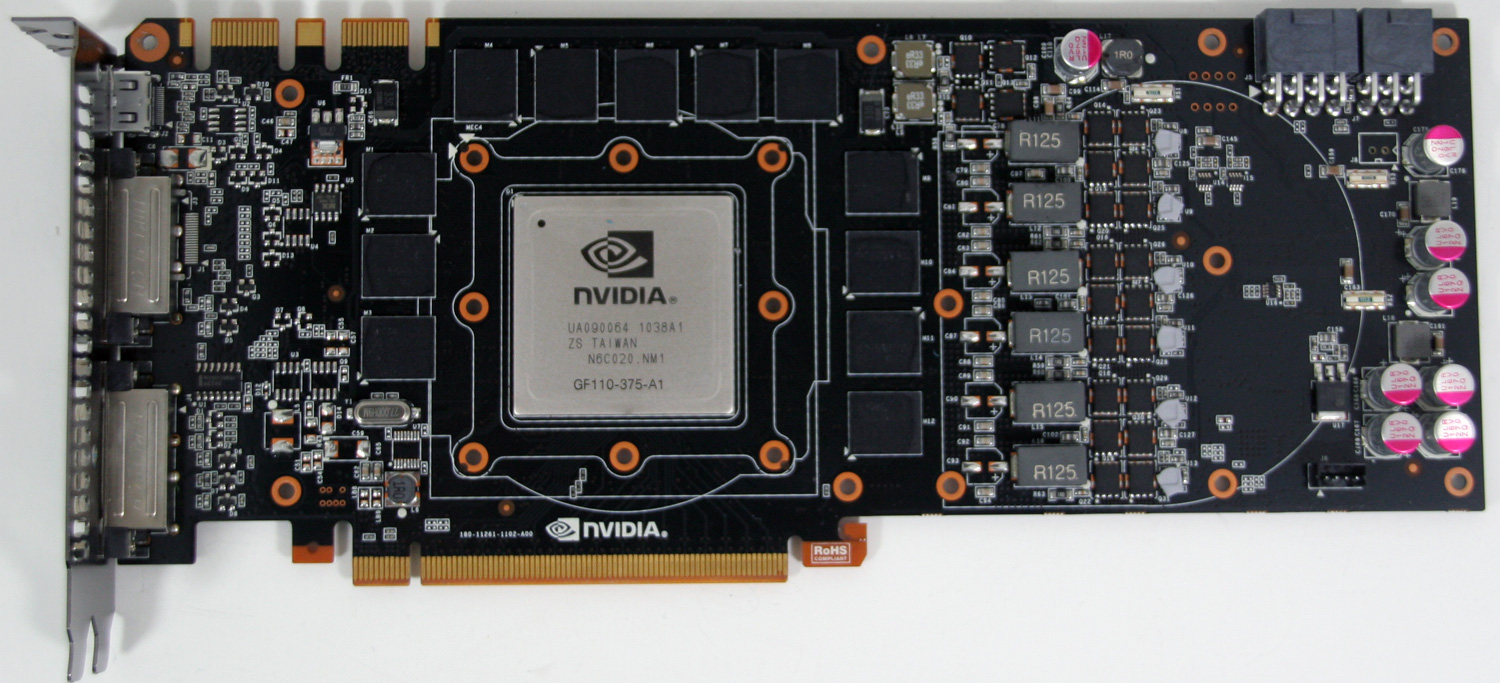
On the front side of the PCB you’ll find the 12 GDDR5 chips composing the card’s 384bit memory bus. The thermal pads connecting the memory to the shroud have once again wiped out the chip markings, so we haven’t been able to determine what these chips are, although we’re confident they’re 5Gbps like in past cards. At the center of the card is the GF110 GPU encased in a metal heatspreader, a common sight for NVIDIA’s high-end GPUs. This is an A1 revision GPU, which in NVIDIA’s counting system means it’s the first tape-out. Elsewhere on the board you’ll find the 2 SLI connectors, providing support for tri-SLI on the 580. All told while the GPU has been refined, the PCB remains largely unchanged from the GTX 480 other than removing the ventilation holes – all of the ICs are in practically the same place, and even the VRM controller is the same.
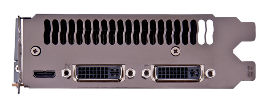
Meanwhile looking at the IO bracket for the 580, we find the same configuration as we saw on the 480. Below a full-sized vent are 2 DVI ports and a mini-HDMI port. NVIDIA slightly revised their display controller for GF110/GTX580; the good news is that HDMI 1.4a is supported, the bad news is that full audio bitstreaming is not supported so it’s the same as it was on the GTX 480: 8 channel LPCM and lossy audio formats like DD+ and DTS. This actually caught us off-guard since we were expecting the full GF104 treatment here, but it just goes to show that this is a GF100-derrivative after all. Unfortunately this also extends to the number of displays supported – NVIDIA still only supports 2 displays on one card, so you need to run in SLI if you intend to take advantage of 3DVision/NVIDIA surround across 3 monitors.
Finally, it’s with some sense of irony that we find ourselves yelling more at AMD than NVIDIA for naming shenanigans this time around, considering it was NVIDIA that brought us the 8800GT/9800GT and GeForce 200/300 product naming snafus. While NVIDIA has made some changes compared to the GTX 480, it’s a very short list; shorter than even AMD’s list for the 6800 series. At the same time, at least the GTX 580 is faster than the GTX 480 versus AMD’s 6800/5800 series. Quite frankly the GTX 580 should be the GTX 485 – the few architectural changes we’ve seen do make a difference, but then NVIDIA did a whole die shrink on the GTX 280 and only got a GTX 285 out of it. Both companies seem committed to coming out with a new family of video cards this year regardless of where the GPU powering them has actually changed. Ultimately the GTX 580 is the second flimsiest excuse for a new series number, next only to simply rebranding an existing GPU.


160 Comments
View All Comments
Sihastru - Tuesday, November 9, 2010 - link
At this point it makes no sense to get rattled up about the 580. We must patiently wait for the 69x0 cards and see what they can bring to the table. I heard rumours of AMD delaying their cards to the end of the year in order to do some "tweaks"...nitrousoxide - Tuesday, November 9, 2010 - link
Delaying is something good because it indicates that Cayman can be very big, very fast and...very hungry making it hard to build. What AMD needs is a card that can defeat GTX580, no matter how hot or power-hungry it is.GeorgeH - Tuesday, November 9, 2010 - link
Is there any word on a fully functional GF104?Nvidia could call it the 560, with 5="Not Gimped".
Sihastru - Tuesday, November 9, 2010 - link
I guess once GTX470 goes EOL. If GTX460 had all it's shaders enabled then the overclocked versions would have canibalized GTX470 sales. Even so, it will happen on occasion.tomoyo - Tuesday, November 9, 2010 - link
My guess is there will be GTX 580 derivatives with less cores enabled as usual, probably a GTX 570 or something. And then an improved GTX 460 with all cores enabled as the GTX 560.tomoyo - Tuesday, November 9, 2010 - link
Good to see nvidia made a noticeable improvement over the overly hot and power hungry GTX 480. Unfortunately way above my power and silence needs, but competition is a good thing. Now I'm highly curious how close the Radeon 69xx will come in performance or if it can actually beat the GTX 580 in some cases.Of course the GTX 480 is completely obsolete now, more power, less speed, more noise, ugly to look at.
7eki - Tuesday, November 9, 2010 - link
What we got here today is a higher clocked, better cooled GTX 480 with a slightly better power consumption. All of that for only 80$ MORE ! Any first served version of non referent GTX 480 is equipped with a much better cooling solution that gives higher OC possibilites and could kick GTX 580's ass. If we compare GTX 480 to a GTX580 clock2clock we will get about 3% of a difference in performance. All thanks to 32 CUDA processors, and a few more TMU's. How come the reviewers are NOW able to find pros of something that they used to criticise 7 months ago ? Don't forget that AMD's about to break their Sweet Spot strategy just to cut your hypocrites tongues. I bet that 6990's going to be twice as fast as what we got here today . If we really got anything cause I can't really tell the difference.AnnonymousCoward - Tuesday, November 9, 2010 - link
32W less for 15% more performance, still on 40nm, is a big deal.7eki - Wednesday, November 10, 2010 - link
32W and 15% you say ? No it isn't a big deal since AMD's Barts GPUs release. Have on mind that GTX580 still consumes more energy than a faster (in most cases) and one year older multi GPU HD5970. In that case even 60 would sound ridiculosly funny. It's not more than a few percent improvement over GTX480. If you don't believe it calculate how much longer will you have to play on your GTX580 just to get your ~$40 spent on power consumption compared to a GTX480 back. Not to mention (again) that a nonreferent GTX480 provides much better cooling solutions and OC possibilities. Nvidia's diggin their own grave. Just like they did by releasing GTX460. The only thing that's left for them right now is to trick the reviewers. But who cares. GTX 580 isn't going to make them sell more mainstream GPUs. It isn't nvidia whos cutting HD5970 prices right now. It was AMD by releasing HD6870/50 and announcing 6970. It should have been mentioned by all of you reviewers who treat the case seriously. Nvidia's a treacherous snake and the reviewers job is not to let such things happen.Sihastru - Wednesday, November 10, 2010 - link
Have you heard about the ASUS GTX580 Voltage Tweak edition that can be clocked up to 1100 MHz, that's more then 40% OC? Have you seen the EVGA GTX580 FTW yet?The fact that a single GPU card is in some cases faster then a dual GPU card built with two of the fastest competing GPU's tells a lot of good things about that single GPU card.
This "nVidia in the Antichrist" speech is getting old. Repeating it all over the interwebs doesn't make it true.