The RV870 Story: AMD Showing up to the Fight
by Anand Lal Shimpi on February 14, 2010 12:00 AM EST- Posted in
- GPUs
The Cost of Jumping to 40nm
This part of the story could almost stand on its own, but it directly impacts much of what happened with Cypress and the entire Evergreen stack that it’s worth talking about here.
By now you’ve most likely heard about issues with TSMC’s 40nm process. While the word is that the issues are finally over, poor yields and a slower than expected ramp lead to Cypress shortages last year and contributed to NVIDIA’s Fermi/GF100 delay. For the next couple of pages I want to talk about the move to 40nm and why it’s been so difficult.
The biggest issue with being a fabless semiconductor is that you have one more vendor to deal with when you’re trying to get out a new product. On top of dealing with memory companies, component manufacturers and folks who have IP you need, you also have to deal with a third party that’s going to actually make your chip. To make matters worse, every year or so, your foundry partner comes to you with a brand new process to use.
The pitch always goes the same way. This new process is usually a lot smaller, can run faster and uses less power. As with any company whose job it is to sell something, your foundry partner wants you to buy its latest and greatest as soon as possible. And as is usually the case in the PC industry, they want you to buy it before it's actually ready.
But have no fear. What normally happens is your foundry company will come to you with a list of design rules and hints. If you follow all of the guidelines, the foundry will guarantee that they can produce your chip and that it will work. In other words, do what we tell you to do, and your chip will yield.
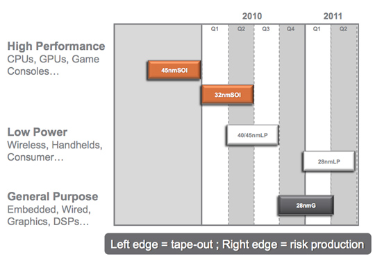
Global Foundries' 2010 - 2011 Manufacturing Roadmap
The problem is that if you follow every last one of these design rules and hints your chip won’t be any faster than it was on the older manufacturing process. Your yield will be about the same but your cost will be higher since you’ll bloat your design taking into account these “hints”.
Generally between process nodes the size of the wafer doesn’t change. We were at 200mm wafers for a while and now modern fabs use 300mm wafers. The transistor size does shrink however, so in theory you could fit more die on a wafer with each process shrink.
The problem is with any new process, the cost per wafer goes up. It’s a new process, most likely more complex, and thus the wafer cost is higher. If the wafer costs are 50% higher, then you need to fit at least 50% more die on each wafer in order to break even with your costs on the old process. In reality you actually need to fit more than 50% die per wafer on the new process because yields usually suck at the start. But if you follow the foundry’s guidelines to guarantee yield, you won’t even be close to breaking even.
The end result is you get zero benefit from moving to the new process. That’s not an option for anyone looking to actually use Moore’s Law to their advantage. Definitely not for a GPU company.
The solution is to have some very smart people in your company that can take these design rules and hints the foundry provides, and figure out which ones can be ignored, and ways to work around the others. This is an area where ATI and NVIDIA differ greatly.


132 Comments
View All Comments
Dudler - Sunday, February 14, 2010 - link
Whoa... Just Whoa.Very insightful and interesting.
Amd moving to GF next generation and Norther Islands this year?
Whoa.
Thx Anand :)
carlhenry - Sunday, February 14, 2010 - link
i really loved the eyefinity being so 'mission impossible'. awesome article!Patrick Wolf - Sunday, February 14, 2010 - link
The first rule of SunSpot: You don't talk about SunSpot. :Dmubeen - Tuesday, February 16, 2010 - link
Such an informative article Mr. Anand. Really appreciate your efforts.just4U - Tuesday, February 16, 2010 - link
I agree it's a great article, nice to see these ones pop up from time to time. It don't really matter to me if it's nvidia, amd or intel.. just having a more insightful read is refreshing.DearSX - Sunday, February 14, 2010 - link
I really do a like article like this. I wonder how old others are cause I'm 25 and I did not even notice how much reading things like this mattered. Its more important than buying something or performance figures imo.Paulman - Sunday, February 14, 2010 - link
I, too, will second that. Really cool. :PMrSpadge - Sunday, February 14, 2010 - link
Many thanks for this interesting article and especially the in-dpeth information about TSMC, the process and how ATI deals with it. Thanks to you, Anand, for writing it and thanks to the good guys at AMD for sharing this information!Beyond excellence :)
hyvonen - Monday, February 15, 2010 - link
And NVidia's call for "zero defects, zero variability" was jaw-dropping. Do they have any idea how silicon is manufactured?Unbelievable cluelessness... with this attitude, they are out of business in the next two years. They are completely unprepared to harness the potential in the latest process nodes.
Meanwhile, it also sounds like TSMC is way over its head in this - uncharacteristic screw-ups with the chamber matching, bad leakage etc. Not to mention the choice to delay HKMG until 28nm (and having to kill 32nm because of that). GF is going to eat them for lunch, and take over the foundry business.
ET - Sunday, February 14, 2010 - link
Indeed. One of the more interesting articles I've read in a while.