The SSD Relapse: Understanding and Choosing the Best SSD
by Anand Lal Shimpi on August 30, 2009 12:00 AM EST- Posted in
- Storage
Live Long and Prosper: The Logical Page
Computers are all about abstraction. In the early days of computing you had to write assembly code to get your hardware to do anything. Programming languages like C and C++ created a layer of abstraction between the programmer and the hardware, simplifying the development process. The key word there is simplification. You can be more efficient writing directly for the hardware, but it’s far simpler (and much more manageable) to write high level code and let a compiler optimize it.
The same principles apply within SSDs.
The smallest writable location in NAND flash is a page; that doesn’t mean that it’s the largest size a controller can choose to write. Today I’d like to introduce the concept of a logical page, an abstraction of a physical page in NAND flash.
Confused? Let’s start with a (hopefully, I'm no artist) helpful diagram:
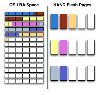
On one side of the fence we have how the software views storage: as a long list of logical block addresses. It’s a bit more complicated than that since a traditional hard drive is faster at certain LBAs than others but to keep things simple we’ll ignore that.
On the other side we have how NAND flash stores data, in groups of cells called pages. These days a 4KB page size is common.
In reality there’s no fence that separates the two, rather a lot of logic, several busses and eventually the SSD controller. The latter determines how the LBAs map to the NAND flash pages.
The most straightforward way for the controller to write to flash is by writing in pages. In that case the logical page size would equal the physical page size.
Unfortunately, there’s a huge downside to this approach: tracking overhead. If your logical page size is 4KB then an 80GB drive will have no less than twenty million logical pages to keep track of (20,971,520 to be exact). You need a fast controller to sort through and deal with that many pages, a lot of storage to keep tables in and larger caches/buffers.
The benefit of this approach however is very high 4KB write performance. If the majority of your writes are 4KB in size, this approach will yield the best performance.
If you don’t have the expertise, time or support structure to make a big honkin controller that can handle page level mapping, you go to a larger logical page size. One such example would involve making your logical page equal to an erase block (128 x 4KB pages). This significantly reduces the number of pages you need to track and optimize around; instead of 20.9 million entries, you now have approximately 163 thousand. All of your controller’s internal structures shrink in size and you don’t need as powerful of a microprocessor inside the controller.
The benefit of this approach is very high large file sequential write performance. If you’re streaming large chunks of data, having big logical pages will be optimal. You’ll find that most flash controllers that come from the digital camera space are optimized for this sort of access pattern where you’re writing 2MB - 12MB images all the time.
Unfortunately, the sequential write performance comes at the expense of poor small file write speed. Remember that writing to MLC NAND flash already takes 3x as long as reading, but writing small files when your controller needs large ones worsens the penalty. If you want to write an 8KB file, the controller will need to write 512KB (in this case) of data since that’s the smallest size it knows to write. Write amplification goes up considerably.
Remember the first OCZ Vertex drive based on the Indilinx Barefoot controller? Its logical page size was equal to a 512KB block. OCZ asked for a firmware that enabled page level mapping and Indilinx responded. The result was much improved 4KB write performance:
| Iometer 4KB Random Writes, IOqueue=1, 8GB sector space | Logical Block Size = 128 pages | Logical Block Size = 1 Page |
| Pre-Release OCZ Vertex | 0.08 MB/s | 8.2 MB/s |


295 Comments
View All Comments
Anand Lal Shimpi - Monday, August 31, 2009 - link
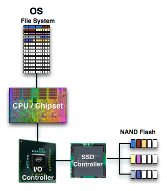
The tables the drive needs to operate are also stored in a small amount of flash on the drive. The start of the circular logic happens in firmware which points to the initial flash locations, which then tells the controller how to map LBAs to flash pages.Take care,
Anand
Bakkone - Monday, August 31, 2009 - link
Any gossip about the new SATA?Zaitsev - Monday, August 31, 2009 - link
Thanks for the great article, Anand! It's been quite entertaining thus far.cosmotic - Monday, August 31, 2009 - link
The page about sizes (GB, GiB, spare areas, etc) is very confusing. It sounds very much like you are confusing the 'missing' space when converting from GB to GiB with the space the drive is using for its spare area.Is it the case that the drive has 80GiB internally, uses 5.5GiB for spare, and reports it's size as 80GB to the OS leaving the OS to say 74.5GiB as usable?
Anand Lal Shimpi - Monday, August 31, 2009 - link
I tried to keep it simply by not introducing the Gibibyte but I see that I failed there :)You are correct, the drive has 80GiB internally, uses 5.5GiB for spare and reports that it has 156,301,488 sectors (or 74.5GiB) of user addressable space.
Take care,
Anand
sprockkets - Tuesday, September 1, 2009 - link
Weird. So what you are saying is, the drive has 80Gib capacity, but then reports it has 80GB to the OS, advertised as having an 80GB capacity, which the OS then says the capacity is 74.5GiB?sprockkets - Tuesday, September 1, 2009 - link
As a quick followup, this whole SI vs binary thing needs to be clarified using the proper terms, as people like Microsoft and others have been saying GB when it really is GiB (or was the GiB term invented later?)For those who want a quick way to convert:
http://converter.50webs.com">http://converter.50webs.com
ilkhan - Monday, August 31, 2009 - link
so they are artifically bringing the capacity down, because the drive has the full advertised capacity and is getting the "normal" real capacity. :argh:Vozer - Monday, August 31, 2009 - link
I tried looking for the answer, but haven't found it anywhere so here it is: There are 10 flash memory blocks on both Intel 160GB and 80GB X25-M G2, right? (and 20 blocks with the G1).So, is the 80GB version actually a 160GB with some bad blocks or do they actually produce two different kind of flash memory block to use on their drives?
Anand Lal Shimpi - Monday, August 31, 2009 - link
While I haven't cracked open the 80GB G2 I have here, I don't believe the drives are binned for capacity. The 80GB model should have 10 x 8GB NAND flash devices on it, while the 160GB model should have 10 x 16GB NAND flash devices.Take care,
Ananad