ASUS Striker II Extreme: Mucho Bang, Mucho Bucks
by Kris Boughton on April 11, 2008 7:00 AM EST- Posted in
- Motherboards
ASUS Striker II Extreme Specifications
| ASUS Striker II Extreme | |
| Market Segment | Ultimate Gamer / Extreme Overclocking - $349.99 (estimated) |
| CPU Interface | Socket T (LGA775) |
| CPU Support | LGA775 Core2 Duo/Extreme/Quad, Pentium EE, Pentium D, Pentium including next-generation 45nm CPU support |
| Chipset | NVIDIA nForce 790i Ultra SLI SPP and MCP (570) |
| CPU Clock Multiplier | 6x ~ 11x, downward adjustable for Core2, upward to 60x for Core2 Extreme, including half-multiplier support for 45nm processors |
| Front Side Bus Speeds | Auto, installed CPU default to 700MHz in 1MHz increments |
| System Bus Speeds | 1600 / 1333 / 1066 / 800 MHz |
| FSB Memory Clock Modes | Auto, Linked, Unlinked |
| DDR3 Memory Ratios | Auto (depends on installed CPU default FSB), 5:4, 3:2 and Sync Mode (2:1) |
| PCIe Speeds | Auto, 100MHz ~ 200MHz in 1MHz
increments PCI 2.0 bus can be adjusted separately from PCI 1.x bus |
| SPP-to-MCP Link Speeds | Auto, 200 ~ 500Mhz in 0.5MHz increments to 210MHz then 1MHz steps |
| HT Multipliers | 1x ~ 5x for SPP->MCP and MCP->SPP |
| EPP 2 Profile Support | Enabled (DDR3-2000 operation), Disabled |
| DRAM Timing Controls | Optimal or Expert (Manual) - tCL, tRCD, tRP, tRAS and CPC |
| Advanced Memory Settings | Auto or Manual - tRRD, tRC, tWR, tWTR, tFAW, tRTP, tRFC and tREF |
| DRAM Command Per Clock | Auto, 1T, 2T |
| MCH P1/P2 Adjustments | Enabled, Disabled |
| CPU Core Control | Enabled, Disabled for each core (excluding Core 0) |
| CPU Voltage | Auto, 1.10000 ~ 2.40000 in 0.00625 increments |
| Loadline Calibration | Enabled, Disabled |
| CPU PLL Voltage | Auto, 1.50V ~ 3.00V in 0.02V increments |
| CPU VTT Voltage | Auto, 1.20V ~ 2.46V in 0.02V increments |
| Memory Voltage | Auto, 1.50V ~ 3.10V in 0.02V increments |
| NB Core Voltage | Auto, 1.30V ~ 2.20V in 0.02V increments |
| SB Core Voltage | Auto, 1.50V ~ 1.85V in 0.05V increments |
| CPU GTLVREF Lane Voltages | Auto, Default, -226mV ~ +224mV for each CPU GTL reference voltage |
| NB GTLREF Lane Voltage | Auto, Default, -126mV ~ +160mV for each CPU GTL reference voltage |
| DDR3 REF Voltages | Auto, Default, -126mV ~ +160mV for each DDR3 channel |
| Memory Slots | Four 240-pin DDR3 DIMM Slots Dual-Channel Memory Architecture Regular Unbuffered, non-ECC DDR3 Memory to DDR3-1333, 8GB Total Supports SLI-Ready EPP 2 Memory to DDR3-2000 |
| Expansion Slots | 2 - PCIe 2.0 x16, supports NVIDIA SLI and Quad-SLI
Technology 1 - PCIe (1.x) x16, allows NVIDIA 3-way SLI with 8800GTX/Ultra 2 - PCIe (1.x) x1, one compatable with audio solution 2 - PCI Slot 2.2 |
| Onboard SATA RAID | 6x SATA 3.0Gbps Ports - nForce MCP (NVIDIA MediaShield RAID 0, 1, 0+1, 5 and JBOD) |
| Onboard IDE/Additional SATA | Jmicron JMB363 SATA Controller (2 external eSATA ports) |
| Onboard USB 2.0/IEEE-1394 | 10 USB 2.0 Ports - (6) I/O Panel, (4) via
headers 2x 1394a Ports - (1) I/O Panel, (1) via header |
| Onboard LAN (with Teaming) | Dual NVIDIA nForce LAN with DualNet and FirstPacket Technology |
| Onboard Audio | 8-channel HD Audio (Azalia) CODEC |
| Power Connectors | ATX 24-pin, 8-pin EATX 12V |
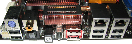
| I/O Panel | 1 x PS/2 Keyboard 2 x SPDIF - (1) Optical Out, (1) Coaxial Out 2 x External eSATA 1 x IEEE-1394a port 2 x RJ-45 (LAN) 6 x USB 2.0 CMOS Reset Button 8 Channel Audio I/O (optional included SupremeFX II Audio Card) |
| Fan Headers | 8 - (1) CPU, (1) Power, (6) Chassis |
| BIOS Revision | 0511 |
Because all 790i (Ultra) boards employ a BIOS based on reference NVIDIA code, we were not surprised to note the many similarities between the ASUS Striker II Extreme and the EVGA 790i offering reviewed at product launch. The Striker II Extreme mostly expands upon the already generous voltage ranges, providing many well beyond the realm of sanity, as well as a couple other switches some may find practical.
Regardless of how you feel about subjecting your 45nm processor to exceedingly high voltages - up to 2.4V minus a nominal droop is possible with this board - more than a few onboard components as well as installed DDR3 memory modules will be damaged if you test the upper limits of each range. To make safeguarding your investments easier we have created this simple to follow voltage limit reference when it comes to overclocking the 790i MCP and a 45nm CPU. Our maximum recommended values are based on safe, reliable, sustained 24/7 operation of each component using either conventional air-cooling or more efficient water-cooling.
Those that plan to pair an older 65nm processor with their 790i motherboard may have a little more margin when it comes to the application of higher CPU core voltages; in this case we would recommend no more than 1.55V. Moreover, the limits listed should be read as maximum in-BIOS selections as these values already take into account any droop in actual voltages. Finally, as a general disclaimer, it is important to recognize that overclocking can subject components to additional stresses that may result in damage, degradation in performance, or even premature failure.
| Voltage Limits | |||
| Highest Voltage Setting Available in BIOS |
Maximum Recommended for Sustained Operation |
Near Instant Damage Occurs at... |
|
| CPU Voltage | 2.40V | 1.50V | 1.80V |
| CPU PLL Voltage | 3.00V | 1.60V | 2.00V |
| CPU VTT Voltage | 2.46V | 1.36V | 2.00V |
| Memory Voltage | 3.10V | 2.00V | 2.40V |
| NB Core Voltage | 2.20V | 1.60V | 2.00V |
| SB Core Voltage | 1.85V | 1.60V | n/a |
Worth noting is that our board disallowed any FSB lower than the installed CPU's default value - a rather odd precept when it comes to overclocking. We would like to see this changed though as there is no obvious benefit to this policy (it only serves to hamper troubleshooting efforts with problems possibly related to higher bus speeds). The Striker II Extreme permits FSB speeds as high as 700MHz, which is more than enough headroom for even extreme overclocking. Reaching such high FSBs is a different story, of course.
Nearly the same as the 790i reference board, PCIe bus interfaces associated with the SPP and MCP can be overclocked separate from one another. Slot 1 and 2 PCIe link resources are provided by the 790i SPP, a PCI Express 2.0 capable part, while Slot 3 hangs off the 570 MCP and conforms to PCI Express 1.x specifications only. The difference is that with the Striker II Extreme, unlike the NVIDIA reference design, PCIe Slot 1 and 2 each receive their master clocking signal from the same physical PLL instead of separate circuits with individual oscillators.
Although we're not absolutely certain, this is perhaps the reason why we were utterly unsuccessful in overclocking the PCIe 2.0 interface with our Striker II Extreme, while the reference design sailed well past 150MHz with relative ease. This was disappointing as earlier testing with the EVGA 790i-based board showed significant 3D performance gains (up to 10%) attributable to this change alone.
Another major drawback with the platform as a whole is the incorporation of an MCP absent a PCIe 2.0 interface, an issue we have been critical of with Intel in the past. Intel's decision to release their X48 Express chipset prior to the availability of their new ICH10(R) Southbridge undoubtedly allowed NVIDIA the opportunity to forgo the design and production of a competitive MCP - making us the real losers in the end.
This may be one of the reasons 3-way SLI shows only moderate gains over traditional 2-way configurations. The addition of a third graphics card theoretically enhances a system's ability to handle larger 3D workloads (provided the CPU power is there), but in most circumstances data transfer constraints imposed by the slower SPP-to-MCP PCIe link inhibit the effective employment of all available GPU resources. It is probably unfair to point finger at Intel for the lack of innovation in NVIDIA products, but it is not far from the truth. When it comes to desktop chipsets, most of the time NVIDIA is simply struggling to keep up with Intel.


23 Comments
View All Comments
seamusmc - Friday, April 11, 2008 - link
For folks considering this board, I strongly recommend visiting xstremesystems.org's forums.Several people are experiencing data/OS corruption when performing any FSB overclocking. (Brings back memories of the early days of the 680i.)
nomagic - Friday, April 11, 2008 - link
LGA775 Core2 Duo/Extreme/Quad, Pentium EE, Pentium D, Pentium including next-generation 45nm CPU supportWhich would include Nehalem, I suppose? Should I also assume that a BIOS update would be required for Nahalem support? Is it possible that a custom board like this might have trouble supporting Nehalem when the times comes?
TemjinGold - Friday, April 11, 2008 - link
No. NOTHING out right now can support Nehalem as that's a completely different socket (different pin count too).