EVGA 680i LT SLI: NVIDIA's 680i Cost Reduced
by Gary Key on March 28, 2007 4:00 AM EST- Posted in
- CPUs
Features and Specifications
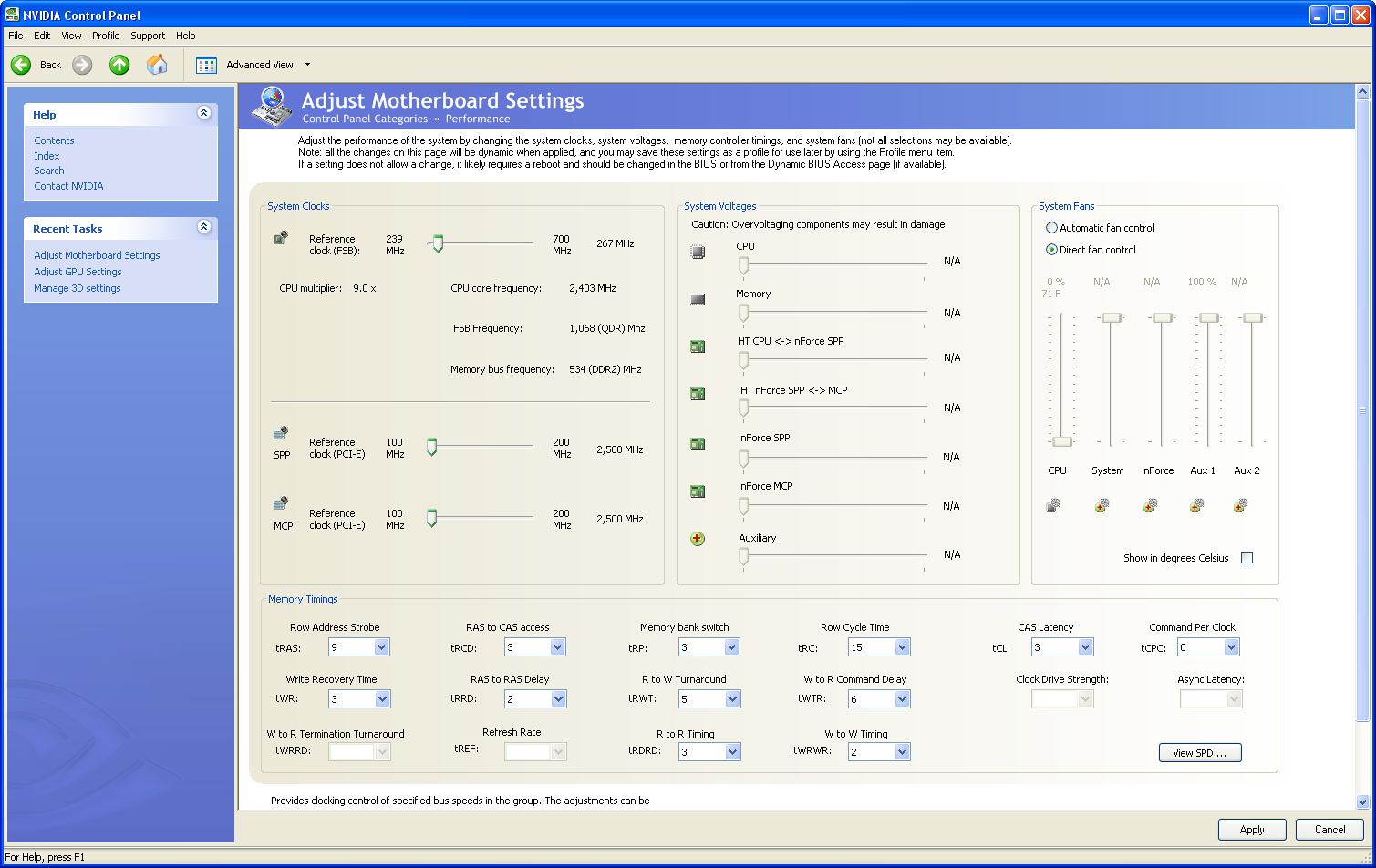
The NVIDIA reference BIOS offers a moderate level of options available for tweaking the board with emphasis placed on the available memory settings. We found in memory testing that switching to manual settings and changing the tCAS, tRCD, tRP, and tRAS was required to ensure optimum performance as our performance results will show shortly.
Compared to the standard 680i BIOS the ability to control the HT and MCP voltages is not available, and FSB and SPP voltages are limited to 1.4V. The inability to change FSB VTT or GTL Ref voltage settings limited our overclocking results to some degree, but more importantly the lack of higher FSB/SPP voltages basically capped our board sample at 500FSB.
One other issue we have with the "Lite" BIOS is that memory voltages are limited to .10V increments meaning that in several cases we could not fine tune our ProMOS or Elpida modules for optimum performance. While we understand NVIDIA's desire not to have this board compete directly with the 680i boards, some of the cuts made are generally frustrating for extracting the best performance out of this board.
EVGA utilizes the standard NVIDIA nTune system utility but in yet another weird BIOS decision the ability to control voltages and fan speeds is non-existent. This ensures that any significant changes required for overclocking the board will have to be done via the BIOS. This is an operation that most people normally do anyway when overclocking, but one of the strengths of NVIDIA's reference boards has been their tight integration with nTune. The inability to control even the CPU fan is inexcusable considering this is a designed by NVIDIA board. Hopefully, the next BIOS release will address these two issues, and we certainly would like see additional voltage controls and automatic fan speed control for the other chassis fan headers. Of course, NVIDIA could really surprise us and offer fan control over the active chipset coolers.
| EVGA 680i LT SLI | |
| Market Segment: | High-End Performance - $199 |
| CPU Interface: | Socket T (Socket 775) |
| CPU Support: | LGA775-based Pentium 4, Celeron D, Pentium D, Pentium EE, Core 2 Duo, Core 2 Extreme |
| Chipset: | NVIDIA 680i LT SPP (C55 P-N-A2) + 680i LT MCP (570 SLI MCP) |
| Bus Speeds: | Auto, 400 to 2500 QDR (100~625) in 1MHz increments |
| Memory Ratios: | Auto, Sync., 1:1, 5:4, 3:2 |
| Memory Speed: | 400MHz~1400MHz in various increments |
| PCIe 1&2 Speeds: | 100MHz~200MHz in 1MHz Increments |
| HT Multipliers: | 1x, 2x, 3x, 4x, 5x |
| Core Voltage: | Auto, 0.80000V to 1.60000 in 0.00625V increments |
| FSB Options: | Auto, Linked, Unlinked |
| CPU Clock Multiplier: | Auto, 6x-11x in 1X increments - Core 2 Duo, downwards unlocked, Core 2 Extreme 6x-60X |
| DRAM Voltage: | Auto, 1.80V to 2.50 in .10V increments |
| DRAM Timing Control: | Optimal, Expert - 10 DRAM Timing Options |
| NB Voltage: | Auto, 1.2V, 1.3V, 1.4V |
| FSB Voltage: | Auto, 1.2V, 1.3V, 1.4V |
| Memory Slots: | Four 240-pin DDR2 DIMM Slots Dual-Channel Configuration, DDR2-400, 533, 667, 800 Regular Unbuffered Memory to 8GB Total |
| Expansion Slots: | 2 - PCIe X16 (2-x16 electrical for SLI or Multi-GPU) 2 - PCIe x1 2 - PCI Slot 2.2 |
| Onboard SATA/RAID: | 6 SATA 3Gbps Ports - 570 SLI MCP (RAID 0,1, 0+1, 5, JBOD) |
| Onboard IDE: | 1 ATA133/100/66 Port (2 drives) - 570 SLI MCP |
| Onboard USB 2.0/IEEE-1394: | 8 USB 2.0 Ports - 4 I/O Panel - 4 via Headers 2 Firewire 400 Ports by TI TSB43AB22A - 1 I/O Panel, 1 via Header |
| Onboard LAN: | NVIDIA Gigabit Ethernet - PCIe - Marvell 88E1116 PHY - 1 port via 570 SLI MCP |
| Onboard Audio: | Realtek ALC885 - 8-channel HD audio codec |
| Power Connectors: | ATX 24-pin, 8-pin EATX 12V, 4-pin 12V Molex |
| I/O Panel: | 1 x PS/2 Keyboard 1 x PS/2 Mouse 1 x S/PDIF Optical - Out 1 x IEEE 1394a 1 x Audio Panel 1 x RJ45 4 x USB 2.0/1.1 |
| BIOS Revision: | Award 721N0P01 |
| Board Revision: | v1.0 |
The NVIDIA reference BIOS offers a moderate level of options available for tweaking the board with emphasis placed on the available memory settings. We found in memory testing that switching to manual settings and changing the tCAS, tRCD, tRP, and tRAS was required to ensure optimum performance as our performance results will show shortly.
Compared to the standard 680i BIOS the ability to control the HT and MCP voltages is not available, and FSB and SPP voltages are limited to 1.4V. The inability to change FSB VTT or GTL Ref voltage settings limited our overclocking results to some degree, but more importantly the lack of higher FSB/SPP voltages basically capped our board sample at 500FSB.
One other issue we have with the "Lite" BIOS is that memory voltages are limited to .10V increments meaning that in several cases we could not fine tune our ProMOS or Elpida modules for optimum performance. While we understand NVIDIA's desire not to have this board compete directly with the 680i boards, some of the cuts made are generally frustrating for extracting the best performance out of this board.
 |
| Click to enlarge |
EVGA utilizes the standard NVIDIA nTune system utility but in yet another weird BIOS decision the ability to control voltages and fan speeds is non-existent. This ensures that any significant changes required for overclocking the board will have to be done via the BIOS. This is an operation that most people normally do anyway when overclocking, but one of the strengths of NVIDIA's reference boards has been their tight integration with nTune. The inability to control even the CPU fan is inexcusable considering this is a designed by NVIDIA board. Hopefully, the next BIOS release will address these two issues, and we certainly would like see additional voltage controls and automatic fan speed control for the other chassis fan headers. Of course, NVIDIA could really surprise us and offer fan control over the active chipset coolers.


16 Comments
View All Comments
Stele - Wednesday, March 28, 2007 - link
It boils down to the engineering headroom put into the PWM design. Let's say the maximum supply current anticipated from a generation of CPUs is 50A (usually from datasheets and/or design guidelines from the CPU manufacturer). Motherboard designers can design their PWM to be just sufficient for this - most notably, the MOSFETs chosen may be those that can handle around 75A - or they can build some headroom in and choose MOSFETs capable of, say, 100A.
The former design philosophy saves cost, and after all it gets the job done. However, since the components would be running near their design limit, they would generate quite a bit of heat... especially during spikes of load and/or when new CPUs with even higher current draw (e.g. quad-core CPUs) show up.
The latter design philosophy is more expensive, but because the components would be running well below their rated spec, they fare much better in terms of thermal dissipation (and hence efficiency, as less power is lost as heat). The lower running temperatures also help improve the reliability of the components since less thermal stresses are present. Furthermore, when current loads increase - be it due to sudden load spikes and/or power-hungry CPUs and/or overclocking - they still have a lot of headroom, and so are able to handle the extra load without breaking a sweat. This results in better stability and again, lower heat dissipation compared to lower-spec'ed components at the same load.
In view of this, perhaps one other area that Anandtech could look at when reviewing motherboards is to have an IR thermometer handy (the ones that you can point and measure temperatures of surfaces remotely with) and perhaps measure the temperatures of the chipset and PWM (or at least the temperatures of their heatsinks) at idle and load. It may not be perfect (especially when heatpiped, and a hotter heatsink could also mean that the heat flow from the component to the heatsink is good due to good thermal contact) but imho at least it would give a useful ballpark figure.
Stele - Wednesday, March 28, 2007 - link
Pretty good review, critically assessing the chipset in light of theory (paper specs) as well as reality (actual value for money based on real-world prices and competiting products).IMHO, Nvidia's attempt to create a lower-cost version of the 680i SLI by limiting BIOS options and tossing the odd feature out (like passive chipset cooling and two USB/one network port) seems a little clumsy at best... Instead, I think the hybrid chipset combination used in, for example, the Asus P5N32-E SLI Plus is a more elegant solution. As this review demonstrated, the BIOS options do not necessarily cap the LT's overclocking capability enough to prevent it from being a threat to the 680i SLI's exclusive turf. Indeed, it might well turn out that the latter's sales would not be jeopardised by the LT anyway - not because of the arbitrarily imposed limitations, but because of the almost non-existent price difference between boards based on the two chipsets, considering the lost features.
Meanwhile, other reviews of the P5N32-E SLI Plus have noted that the MCP used is that from the AMD-platform 590 SLI chipset. I wonder if, other than the slight rearrangement of PCI-Express lanes, there are any real differences (e.g. revised/improved networking/disk controller engines etc) between the two MCPs? Or are these blocks nothing more than carried over directly from the 590 SLI? It would be great if Anandtech could look into that.
Lastly, a tiny note - it's a little amusing to note how it must be a bit pedantic to have to spell out the full name of the 'solid' capacitors used... at least Anandtech strives hard to get it right! :) Really, though, for the kind of 'solid' capacitors that we're talking about on most motherboards, "aluminium solid electrolytic capacitors" or even just "solid electrolytic capactitors" (vs. 'regular' (liquid) electrolytic) would do perfectly. Conductive polymer capacitors are generally (though not restricted to) the little rectangular ones such as the ones seen on Asus RoG boards as well as the P5N32-E SLI Plus. Just a thought :)
yyrkoon - Wednesday, March 28, 2007 - link
Well, about the capacitors, I know as per some OEM, anandtech was calling them 'solid state capacitors', which you sound like you know enough about electronics to know this is wrong. Anyhow, several readers, including myself called 'foul', and there you have it . . .JarredWalton - Wednesday, March 28, 2007 - link
There were a few complaints when he used "solid capacitors", so I guess the full name is the safe way to go. LOLStele - Wednesday, March 28, 2007 - link
Oh very true! "Solid capacitors" and "solid state capacitors" (as yyrkoon rightly commented) are both commonly used on many hardware sites, and are both inaccurate. One reason for the repeated complaints, iirc, is that we were simply oscillating between one inaccurate term and another. :P"Solid electrolytic capacitors"... now that is perfectly acceptable, despite a difference of one word. The devil, as they say, is in the details. ;)
yyrkoon - Wednesday, March 28, 2007 - link
You did the right thing Jarred, you know how picky 'us' readers are ;)