AMD Zen 3 Ryzen Deep Dive Review: 5950X, 5900X, 5800X and 5600X Tested
by Dr. Ian Cutress on November 5, 2020 9:01 AM ESTSection by Andrei Frumusanu
The New Zen 3 Core: Load/Store and a Massive L3 Cache
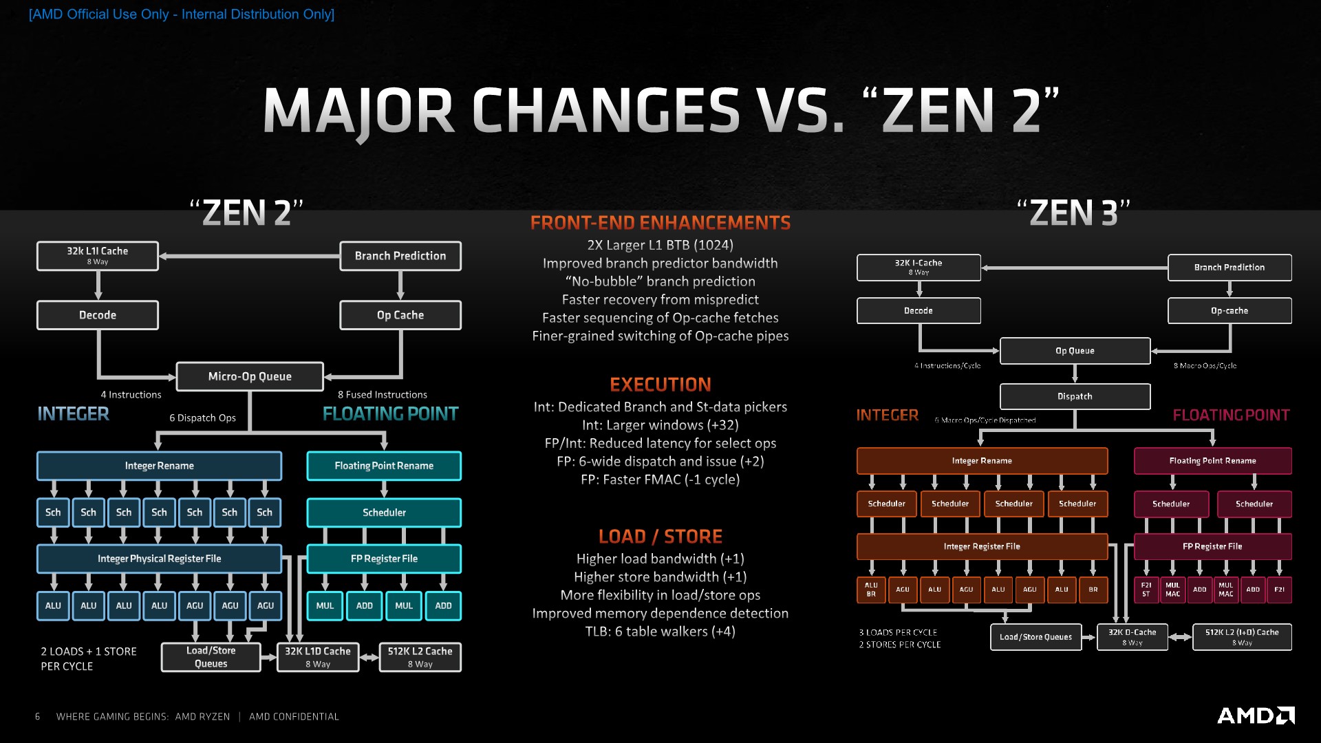
Although Zen3’s execution units on paper don’t actually provide more computational throughput than Zen2, the rebalancing of the units and the offloading of some of the shared execution capabilities onto dedicated units, such as the new branch port and the F2I ports on the FP side of the core, means that the core does have more actual achieved computational utilisation per cycle. To be able to make sure that memory isn’t a bottleneck, AMD has notably improved the load/store part of the design, introducing some larger changes allowing for some greatly improved memory-side capabilities of the design.
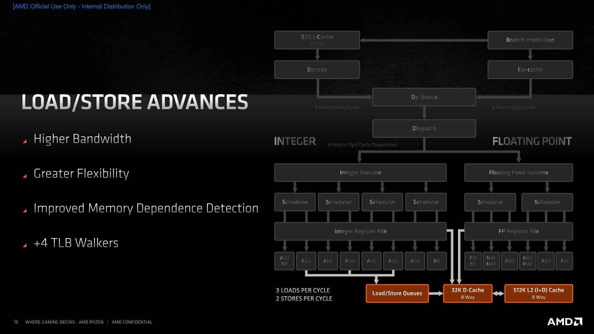
The core now has a higher bandwidth ability thanks to an additional load and store unit, with the total amount of loads and stores per cycle now ending up at 3 and 2. AMD has improved the load to store forwarding to be ablet to better manage the dataflow through the L/S units.
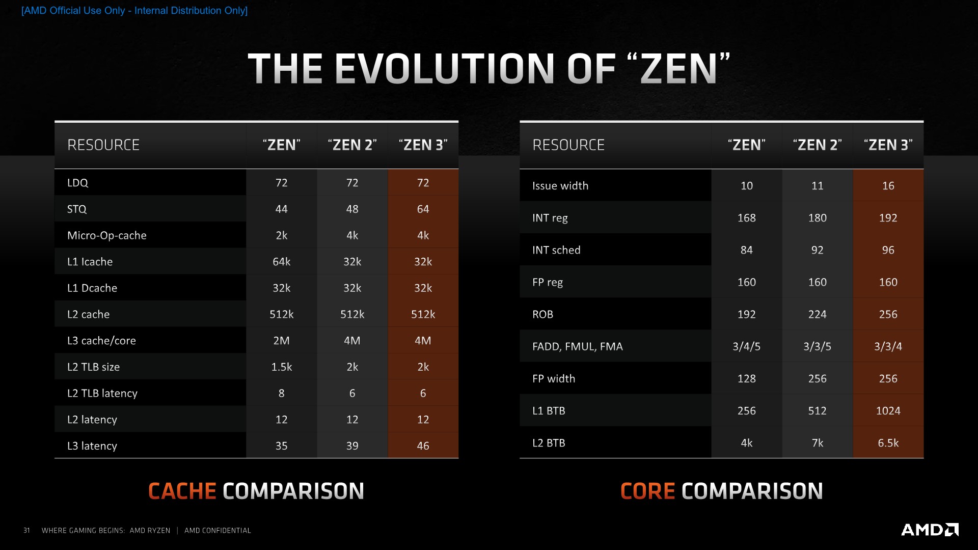
An interesting large upgrade is the inclusion of 4 additional table walkers on top of the 2 existing ones, meaning the Zen3 cores has a total of 6 table walkers. Table-walkers are usually the bottleneck for memory accesses which miss the L2 TLB, and having a greater number of them means that in bursts of memory accesses which miss the TLB, the core can resolve and fetch such parallel access much faster than if it had to rely on one or two table walkers which would have to serially fulfil the page walk requests. In this regard, the new Zen3 microarchitecture should do significantly better in workloads with high memory sparsity, meaning workloads which have a lot of spread out memory accesses across large memory regions.
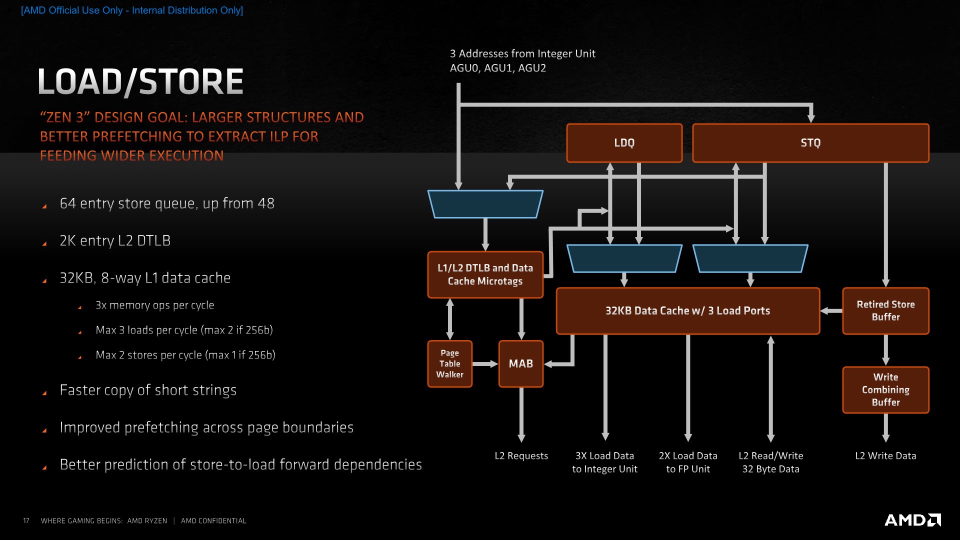
On the actual load/store units, AMD has increased the depth of the store queue from 48 entries to 64. Oddly enough, the load queue has remained at 44 entries even though the core has 50% higher load capabilities. AMD counts this up to 72 by counting the 28-entry address generation queue.
The L2 DTLB has also remained at 2K entries which is interesting given that this would now only cover 1/4th of the L3 that a single core sees. AMD explains that this is simply a balance between the given performance improvement and the actual implementation complexity – reminding us that particularly in the enterprise market there’s the option to use memory pages larger than your usual 4K size that are the default for consumer systems.
The L1 data cache structure has remained the same in terms of its size, still 32KB and 8-way associative, but now seeing an increase in access concurrency thanks to the 3x loads per cycle that the integer units are able to request. It doesn’t actually change the peak bandwidth of the cache as integer accesses can only be 64b for a total of 192b per cycle when using 3 concurrent loads – the peak bandwidth is still only achieved through 2 256b loads coming from the FP/SIMD pipelines. Stores similarly have been doubled in terms of concurrent operations per cycle, but only on the integer side with 2 64b stores, as the FP/SIMD pipes still peak out at 1 256b store per cycle.
REP MOVS instructions have seen improvements in terms of its efficiencies for shorter buffer sizes. This means that in contrast to past microarchitectures which might have seen better throughput with other copy algorithms, on Zen3 REP MOVS will see optimal performance no matter how big or small the buffer size being copied is.
AMD has also improved their prefetchers, saying that now patterns which cross page boundaries are better detected and predicted. I’ve noted also that the general prefetcher behaviours have dramatically changed, with some patterns, such as adjacent cache lines being pulled into L1, something which is very aggressive, and also more relaxed behaviour, such as some of our custom pattern no longer being as aggressively picked up by then new prefetchers.
AMD says that the store-to-load forwarding prediction is important to the architecture and that there’s some new technology where the core is now more capable of detecting dependencies in the pipeline and forwarding earlier, getting the data to instructions which need them in time.
A Big Fat 32MB L3 Cache
Moving out from the individual cores, we come to the brand-new 32MB L3 cache which is a cornerstone characteristic of the new Zen3 microarchitecture and the new Ryzen 5000 CCD:
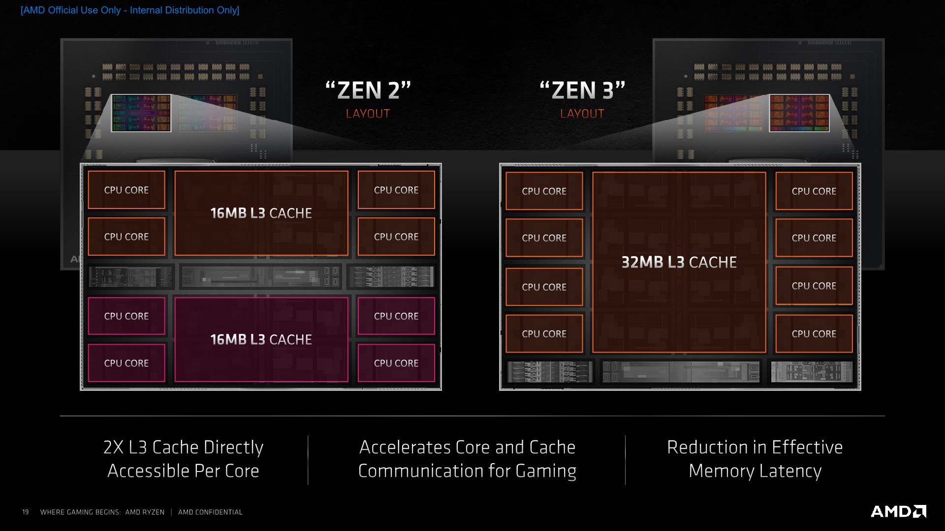
The big change here is of a topological nature, as AMD does away with the 4-core CCX which had been previously used as the unified core cluster block for Zen/Zen+/Zen2. Instead of having to divide a chiplet’s total cache capacity into two blocks of 4 and 4 cores, the new unified L3 aggregates the previously laid out SRAM amount into a single large 32MB pool spanning 8 cache slices and servicing 8 cores.
Achieving this larger 32MB L3 cache didn’t come without compromises as latencies have gone up by roughly 7 cycles to 46 cycles total. We asked AMD about the topology of the new cache but they wouldn’t comment on it besides stating that it’s still an address-hash based system across the 8 cache slices, with a flat memory latency across the depth of the cache, from the view of a single core.
One thing that AMD wasn’t able to scale up with the new L3 cache is cache bandwidth – here the new L3 actually features the same interface widths as on Zen2, and total aggregate bandwidth across all the cores peaks out at the same number as on the previous generation. The thing is now, the cache serves double the cores, so it means that the per-core bandwidth has halved this generation. AMD explains is that also scaling up the bandwidth would have incurred further compromises, particularly on the power side of things. In effect this means that the aggregate L3 bandwidth on a CCD, disregarding clock speed improvements, will be half of that of that of a Zen2/Ryzen 3000 CCD with two CCX’s (Essentially two separate L3’s).
The net win of the new structure from greatly improved cache hit rates for application with larger memory pressures, taking advantage of the full 32MB L3, as well as workloads which make use of heavy synchronisation and core-to-core data transfers: Whereas in previous generations two cores in different CCX’s on the same die would have to route traffic through the IOD, this on-die penalty is completely eliminated on Zen3, and all cores within the new CCD have full and low-latency communication to each other through the new L3.
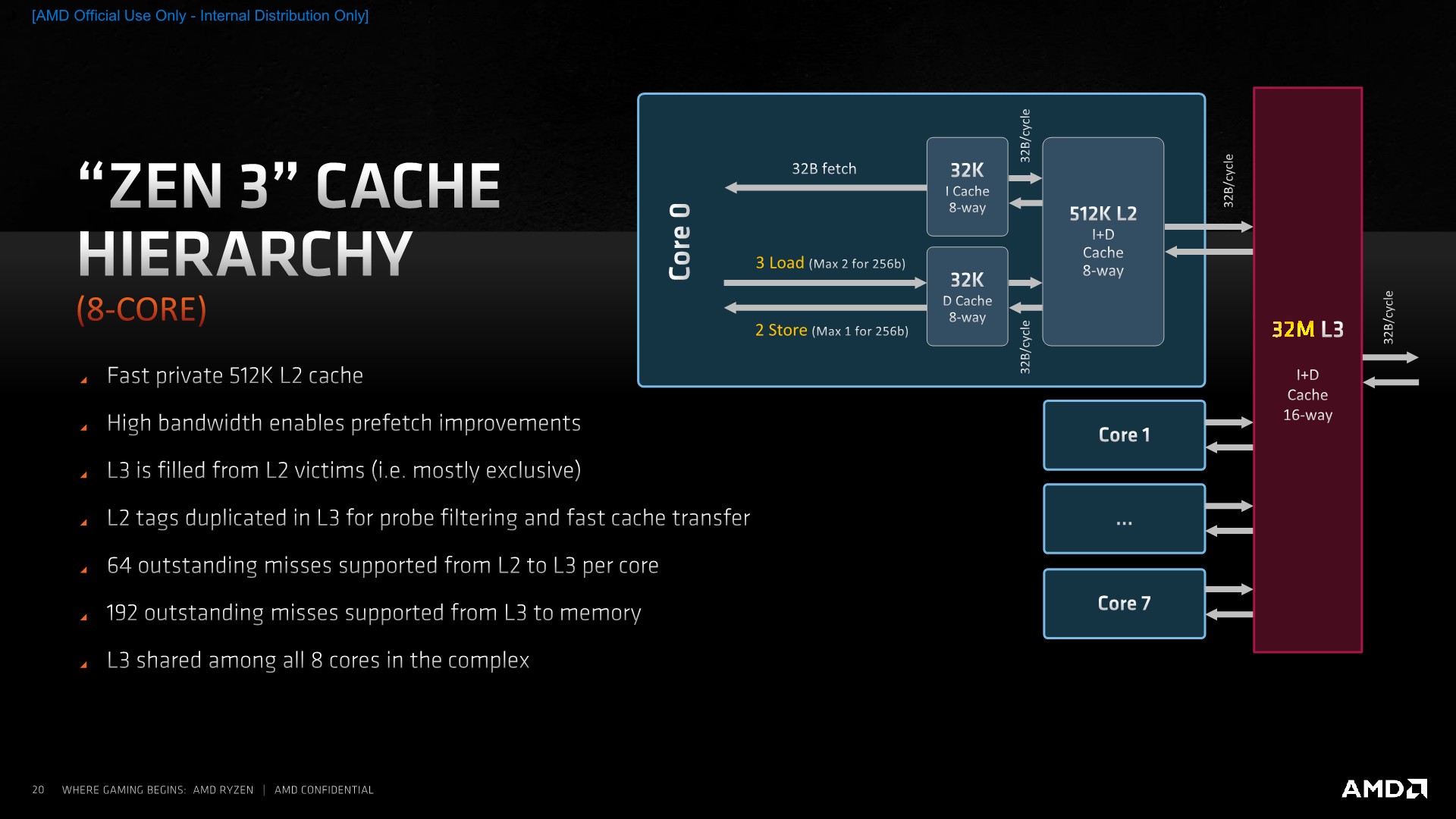
Viewing the whole cache hierarchy on the new Zen3 design, we see a somewhat familiar picture. The L2’s have remained unchanged at 512KB and a 12-cycle access latency, with the memory interfaces from the L1D to through to the L3 coming in at 32B/cycle both in reads and writes.
The L3 continues to maintain shadow tags of the cores’ L2 contents – so if a cache line is requested by one core and resides on another core in the new core complex, the L3 will know from which core to fetch that line back from.
In terms of parallelism, there can be up to 64 outstanding misses from the L2 to the L3, per core. Memory requests from the L3 to DRAM hit a 192 outstanding miss limit – which actually might be a bit low in scenarios where there’s a lot of cores accessing memory at the same time. This is a doubling from the 96 outstanding misses per L3 on Zen2, so the misses per core ratio here at least hasn’t changed.
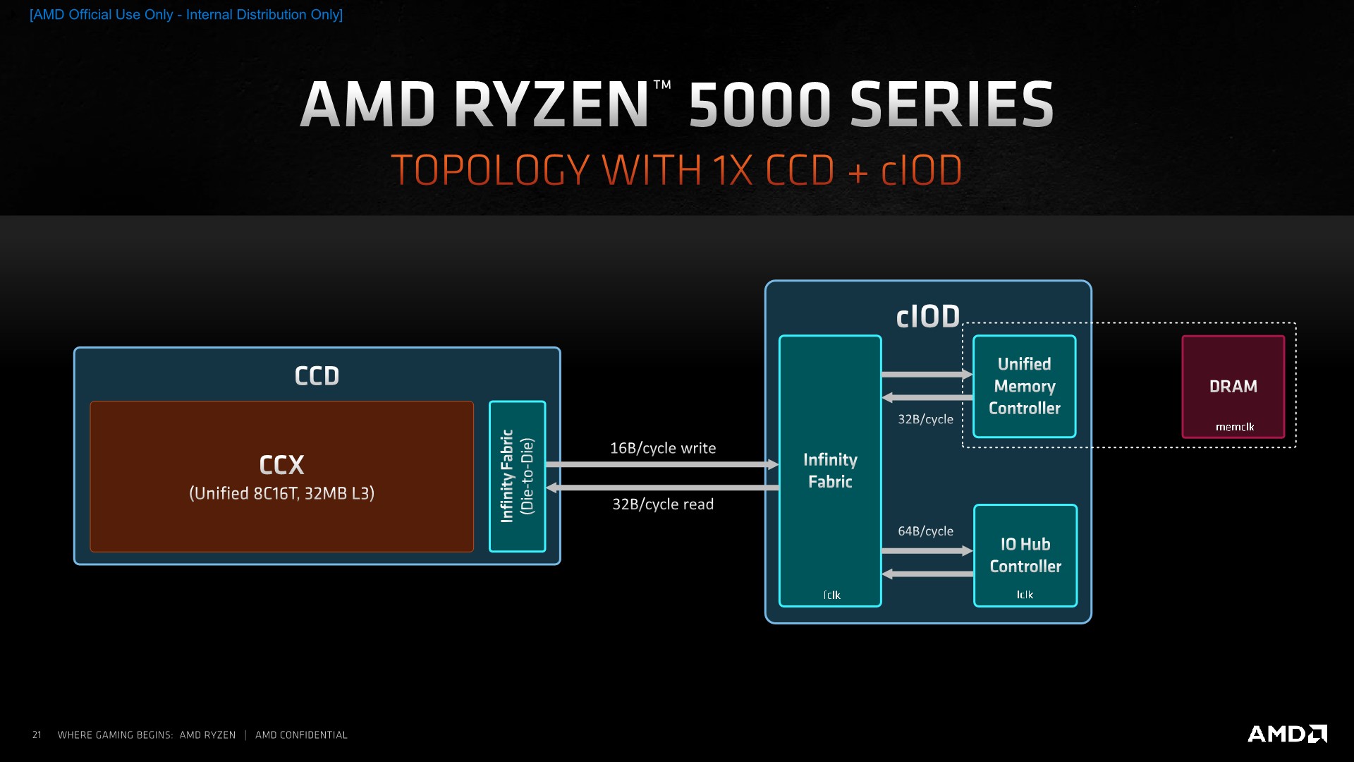
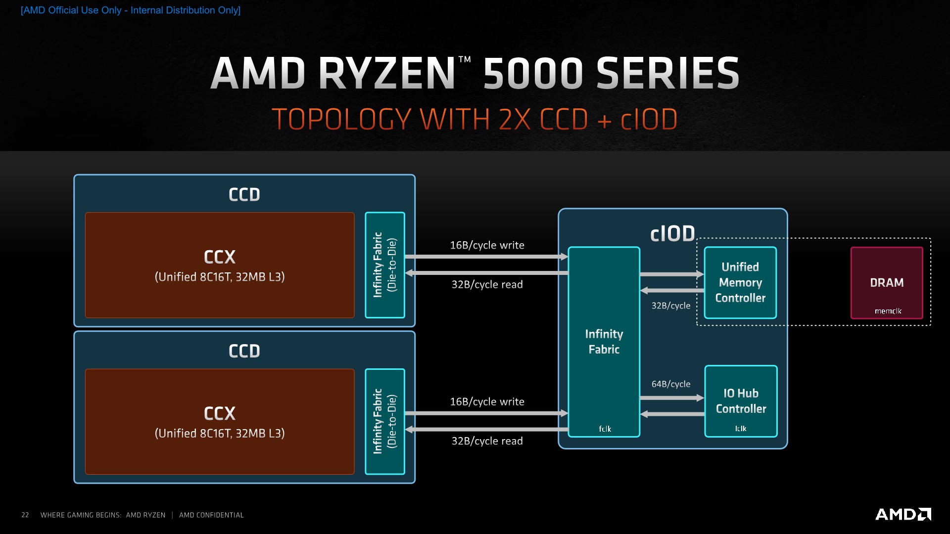
In terms of the packaging topology, because the new Ryzen 5000 series are using the same IOD as the Ryzen 3000 series, we don’t actually see any change in the overall structure of the design. We can either have SKUs with only a single chiplet, such as the new Ryzen 5 5600X or Ryzen 7 5800X, or deploy two chiplets, such as the Ryzen 9 5900X or Ryzen 9 5950X.
The bandwidth between the CCD and the IOD remains the same between generations, with 16B/cycle writes from the CCD to the IOD, and 32B/cycle reads in the opposite direction. Infinity fabric speed is the determining factor for the resulting bandwidth here, which AMD still recommends to be coupled 1:1 with DRAM frequency for the best memory latency, at least until around DDR4-3600, and slightly above for overclockers.
While we’ll be covering the end-performance and actual IPC improvements of Zen3 in the following pages, the first impressions based on AMD’s microarchitectural disclosures are that the new design is indeed a larger-than-average effort in the company’s CPU roadmap.
AMD calls Zen3 a ground-up redesign or even a clean-sheet design. Whilst that seems a quite lofty description of the new microarchitecture, it’s true that at least the architects have touched a lot of aspects of the design, even if at the end a lot of the structures and actual overall width of the core, especially on the front-end, hasn’t actually changed all that much from Zen2.
My view of what Zen3 is, is that it’s a rebuild of the previous generation, with AMD taking lessons from the past implementation and improving and refining the overall broader design. When asked about future potential for widening the core, similarly to some of the current competing microarchitectures out there, AMD’s Mike Clarke admitted that at some point they will have to do that to make sure they don’t fall behind in performance, and that they are already working on another future clean-sheet redesign. For the time being, Zen3 was the right choice in terms balancing out performance, efficiency, time-to-market, as well as considering that this generation actually didn’t have a large process node uplift (Which by the way, will be a rarer and increasingly unreliable vector for improving performance in the future).
I do hope that these designs come in a timely fashion with impressive changes, as the competition from the Arm side is definitely heating up, with designs such as the Cortex-X1 or the Neoverse-V1 appearing to be more than a match for lower-clocked Zen3 designs (such as in the server/enterprise space). On the consumer side of things, AMD appears to be currently unrivalled, although we’ll be keeping an eye open for the upcoming Apple silicon.


339 Comments
View All Comments
LithiumFirefly - Friday, November 6, 2020 - link
I thought the whole point to a civilization game benchmark was a time to complete turn not FPS who cares about FPS and a turn-based game.dagobah123 - Friday, November 6, 2020 - link
The more benchmarks the better. These are general purpose CPUs. Wouldn't it be a shame if you bought a 120hz+ 4k monitor with an expensive graphics card, only to find out your CPU was limiting your frames? Sure the game is playable @ 5 FPS as the author mentioned. However, it's getting harder to make the CPU the bottleneck in a lot of these games at higher resolutions and quality settings, so they have to resort to this. Would anyone play a game @ 360p? No, but if you want to see which CPU is better I say lets include every benchmark we can find.CookieBin - Friday, November 6, 2020 - link
I find it funny that these huge gains mean literally nothing at 4K. So all these different review sites highlight sky high fps at 1080p because at 4K that huge advantage becomes less than a 0.3% improvement.. keep pounding sand linus tech tips. I've never seen such a big nothing burger. No idiot out there buys a $800 5950X to play video games at 1080p.chuyayala - Friday, November 6, 2020 - link
The reason they test 1080p is because game processing is CPU-bound at that resolution (they are testing the CPU after-all). The higher the resolution, the more the GPU is working (not the CPU). The reason why there aren't much gains in 4k is because processing is limited by the GPU power. If we assume we get ultra powerful GPUs that can run 4k games at 120+ frames per second, then the CPU becomes more important.dagobah123 - Friday, November 6, 2020 - link
This is simply not true. It only appears to 'mean nothing' if you don't realize the bottleneck in the testing system on most of the benchmarks are the GPU. Meaning the GPU is maxed out at 100%. In this case you're right, the difference between many CPUs will not matter, but what about next year when you decide to buy the next high-end GPU, only to find out the CPU you choose couldn't handle much more. This is why 360p, 720p, even 1080p benchmarks are included to show you just how much more ahead one CPU is over another. Check out the test setup--they are using a 2080 Ti. Come check out the updated reviews after they test all this on 3090s and 6900 XTs.Pit a Ferarri and a Ford Model T against one another. Sure they both keep up with one another in the grocery parking lot @ 15mph. Take em out on the freeway with a 70mph speed limit and you'll have a clear winner. Let alone let em loose on the race track.
Future proof yourself a bit, buy a 5600k or 5800k for your 4k gaming. If you don't update your CPU often you'll be glad you did a couple years out if you drop in that next GPU.
nandnandnand - Saturday, November 7, 2020 - link
5950X will make your web browsing snappier... so you can load more AnandTech ads. ;)zodiacfml - Sunday, November 8, 2020 - link
duh? Steam survey shows 1080p the most popular resolution for gaming. Aside from that, it is difficult to maintain frame rates for 240Hz/360Hz monitors.You might have a point with 720p res though
realbabilu - Friday, November 6, 2020 - link
First: I think you should compare with F or KF Intel version, for price comparison. Since they don't have internal Gpu. Somehow AMD not included the FAN also, beware good cooling isn't cheap.SECOND: it's nice to had coding bench with optimization here windows, with AVX2 and some flags compiling, Amd only provide optimization compiling on Linux only, I think they should be on windows too with optimized math kernel and compiler.
ThIrd: the price performance is justified now. In zen2 release the price was lower than Intel that time, made Intel justified the price for 10th Gen. Now from price sensitive, Intel still fine per price / performance ratio,even though it's need more power consumption.
duploxxx - Saturday, November 7, 2020 - link
the ryzens have a base TDP of 105W and peaking towards 140-150Wnot like the intels that peak at +200ish W, there you need good cooling.
A Dark rock slim or shadow rock can easily handle this and it will cost you 50-60$..
go find a cooler for the +200W so that it wont throttle all the time for the Intel
realbabilu - Saturday, November 7, 2020 - link
Great. I think Anand tech should do cooling shootout for 5900x/5950x bench.To find the minimum air cooler for this,
AMD only list noctua and bequiet as air cooler, others as liquid cooler at https://www.amd.com/en/processors/ryzen-thermal-so...
The slim rock and nh14s maybe the cheapest on the list. It is interesting could more budget double fan tower should enough for 5900x/5950x that has 145 watt max like deepcool gammax 400 pro (double fan), coolermaster ma410p, and shadow rock 2/3, and maybe cheapest aio coolermaster liquid master 120 lite that not listed on amd list.