The Apple iPhone 11, 11 Pro & 11 Pro Max Review: Performance, Battery, & Camera Elevated
by Andrei Frumusanu on October 16, 2019 8:30 AM ESTThe A13's Memory Subsystem: Faster L2, More SLC BW
The memory subsystem of a chip is an essential backbone for the performance of not only the CPU cores, but also the whole rest of the system. In this case we’re taking a closer look at how the memory subsystem behaves on the CPU side of things.
Last year we saw Apple make significant changes to the SoC’s memory subsystem with the inclusion of a new architecture system level cache (SLC), which serves as the last level cache for not only the CPU, but also a lot of other SoC components like the GPU.
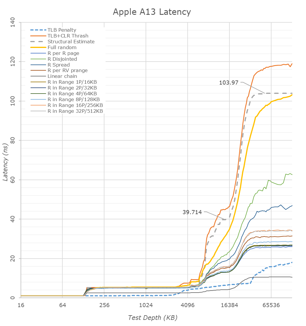
Looking first at the linear graphed memory latencies, we see that the A13’s structural DRAM latency falls in at ~104ns, a very slight regression to the 102.8ns of the A12. Apple in this regard isn’t the best among mobile SoCs, HiSilicon’s newest Kirin 990 now falls in at ~96ns and the Exynos 9820 should also fall into a similar range, however this doesn’t matter too much in the grand scheme of things given Apple’s massive cache hierarchy. Patterns such as full random pointer chasing is significantly more performant on Apple’s cores and this should be tightly linked to the strong TLBs as well as iOS’s system configuration choice of using 16KB pages.
Moving to a logarithmic chart we better see the transitions between the cache hierarchies. We can clearly see Apple’s 128KB L1D cache here. The L2 cache is also relatively straightforward till 4MB as the latencies are relatively flat. From here on things become quite complicated and things differ a bit compared to the A12. Last year we determined that the L2 cache structure physically must be around 8MB in size, however we saw that it only looks as if the big cores only have access to around 6MB. Apple employs an “L2E” cache – this is seemingly a region of the big core L2 cache that serves as an L3 to the smaller efficiency cores (which themselves have their own shared L2 underneath in their CPU group).
In this region the new A13 behaves slightly different as there’s an additional “step” in the latency ladder till about 6MB. Frankly I don’t have any proper explanation as to what the microarchitecture is doing here till the 8MB mark. It does look however that the physical structure has remained at 8MB.
Going further out into the cache hierarchy we’re hitting the SLC, which would act as an L3 to the large performance cores, but should be shared with other IP blocks in the SoC. Here we see a significant change in behavior to the A12. If one had to guess as to what happening you’d think that the SLC has grown in size beyond the 8MB we estimated to have been used in the A12. Short of analyzing the die shot and see if the structure indeed has doubled, I’m a bit skeptical and I feel it’s more likely that Apple is using a partitioning system and has possibly enabled the CPU complex to access more of the SLC. What is evident here, is the doubling of the SLC cache from 8MB to 16MB.
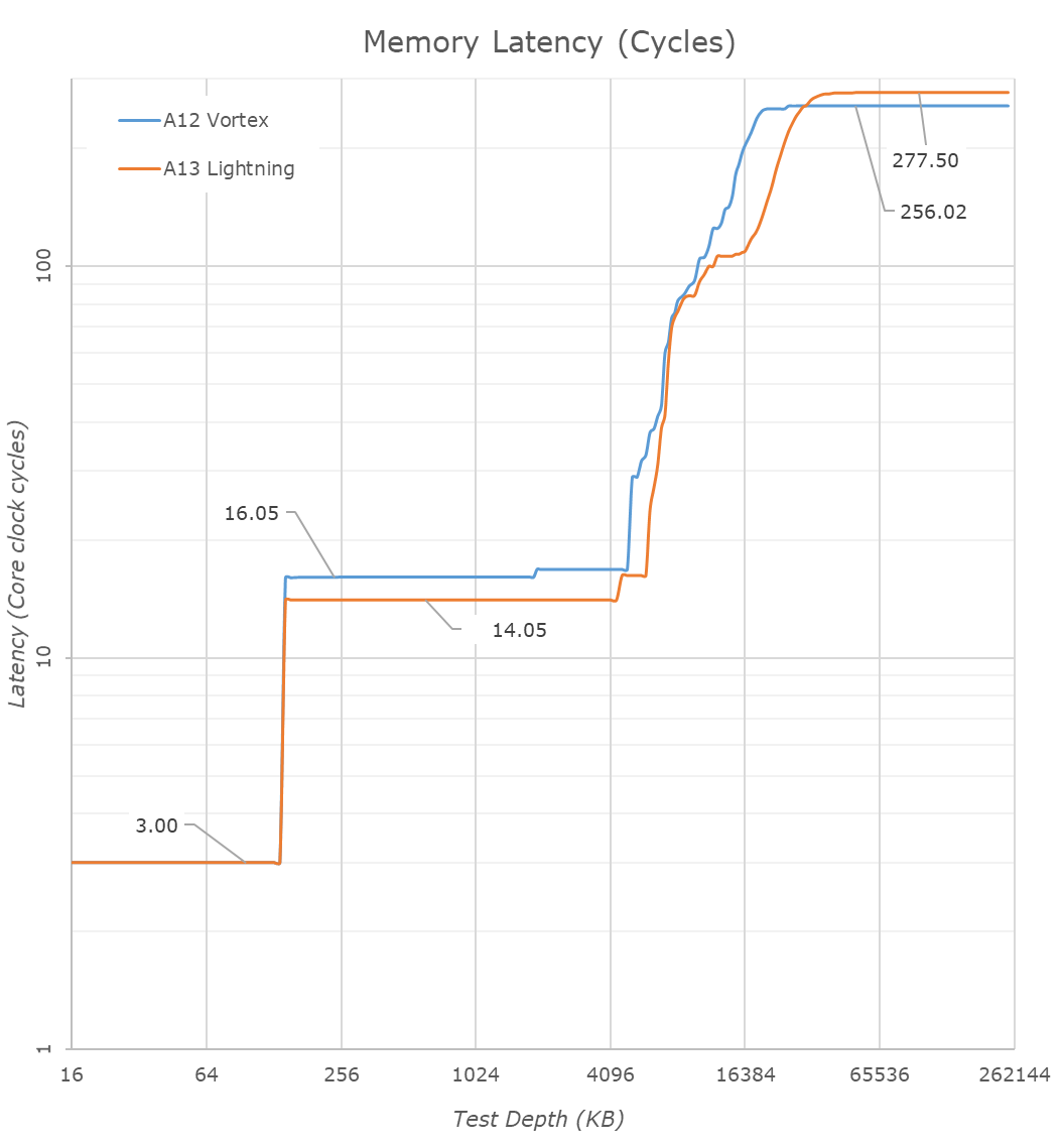
We mentioned that the Lightning cores L2 is faster now: Converting the measured latencies from nanoseconds to core cycles, we see the structural speed changes to the caches. The L1 remains at 3 cycles which is massively impressive given its 128KB size. The L2 cache has been reduced from 16 cycles down to 14 cycles, which is again extremely impressive given its purported 8MB physical size. Accounting for the core’s frequency increase, we do more noticeably see that the structural memory latency has increased a bit on the A13, adding about 21-22 cycles. It’s possible that the microarchitectural changes that made the SLC so much faster this generation had a knock-on effect in adding more total latency to DRAM.

Looking at the new Thunder cores versus last year’s Tempest microarchitecture, we see the new cache hierarchy differences. The L1D has grown from 32KB to 48KB – straightforward until now.
The L2 cache size also has evidently increased. Last year we estimated that the small core cluster had 2MB of shared L2, but was partitioned in such as way that a given core only has access to about 1.5MB, and this depth depended on the power management policy and DVFS state of the cores, appearing to only have access to 512KB when at the lowest performance states.
This year, this 1.5MB access size has seemingly increased to 2.5MB. I thus estimate the shared L2 of the small cores has increased from a physical 2MB to 3MB. Past this we’re seeing a step-wise behavior in latency up to 4MB – it’s possible this would be part of the L2E cache of the CPU complex, so in other words we’d possibly be accessing a special partition of the big core’s L2.
Update October 27th: The die shot reveals that the L2 of the Thunder cluster is half the size of the Lightning cluster L2, thus we estimate it's 4MB large in total.
In this graph we continue to see the behavior change of the A13’s SLC. At first glance it appears bigger, which still can be the case, but I rather think the CPU complex has much better access to the 4 (or more) cache slices of the SLC in this generation.
Another change of the new Thunder cores here is that we’re obviously seeing an increase in the L2 TLB capacity of the core. While the L1 TLB seems to have remained unchanged at 128 pages / 2MB, the L2 TLB has increased from 512 pages to 1024 pages – covering up to 16MB, a quite ideal size as it’s covering the depth of the SLC.
Finally, we see that the efficiency cores in the A13 this time around don’t have access to faster DRAM on their own – the memory controller remains very slow and DRAM latencies are in excess of 340ns while on the A12 the Tempest cores were able to enjoy latencies of 140-150ns. This explains some of the performance regressions of the new Thunder cores we measured earlier.
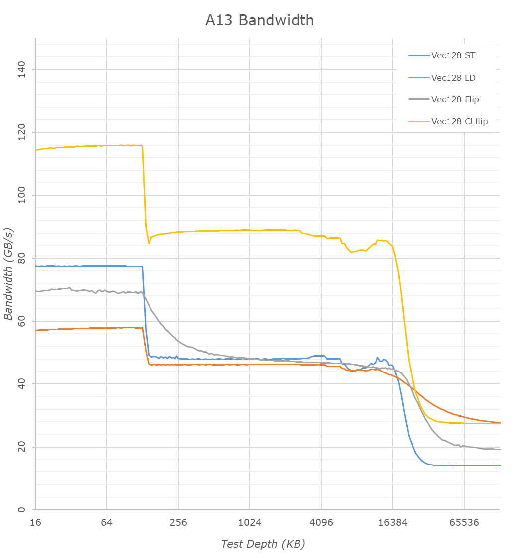
Bandwidth between the A13 and A12 doesn’t majorly differ in the L1 and DRAM regions beyond minor clock speed changes. In the L2, we notice there’s been a more noticeable increase in performance for read+writes into the same cache line, increasing performance by 25%.
It’s again in the SLC region where we see major changes – while on the A12 the bandwidth here slowly fell off in depth, the A13 is able to sustain the same bandwidth over the 16MB of system cache. It’s impressive that the bandwidth here is essentially equal to the L2 – albeit of course quite notably worse latency as we noted earlier. The smaller dips at the 8MB region is an artifact of the cache behavior between the big L2 and the SLC.
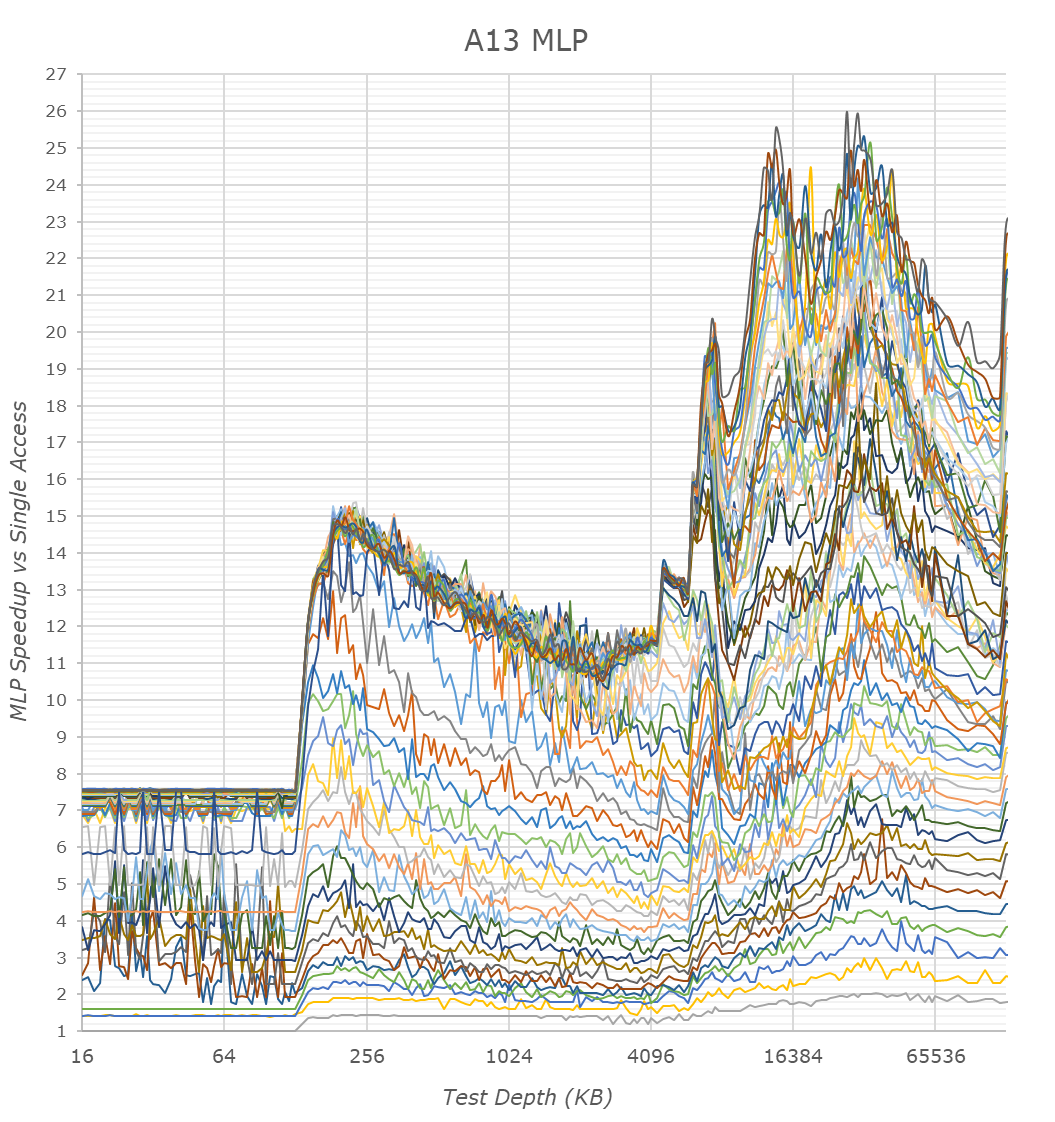
Finally, the MLP graphs showcase the memory level parallelism capacity of the CPU cores and the memory subsystem. MLP is the ability for the CPU to “park” memory requests missing the caches and to continue executing in out-of-order fashion other requests. High MLP ability is extremely important to be able to extract the most from out-of-order execution of code, which has higher memory pressure and more complex memory access patterns.
The A13 here again remains quite unique in its behavior, which is vastly more complex that what we see in any other microarchitecture. The non-linearity of the MLP speedup versus access count is something I can’t find a viable explanation for. We do see that the new A13 is a little bit better and more “even” than the A12, although what this practically means is something only Apple’s architects know. In general, Apple’s MLP ability is only second to AMD’s Zen processors, and clearly trounces anything else in the mobile space.
The overall conclusion for the A13’s memory subsystem is that Apple has evidently made very large changes to the system level cache, which is now significantly faster than what we’ve seen in the A12. The L2 cache of the big cores benefit from a 2-cycle latency reduction, but otherwise remain the same. Finally, the new Thunder efficiency cores have seen large changes with increased L1D, L2 and TLB capacity increases.


242 Comments
View All Comments
FunBunny2 - Thursday, October 17, 2019 - link
"I wonder which workloads can it possibly affect."lots and lots of software fake floating point arithmetic by scaling integer arithmetic. way faster, even counting the need to shift the decimal point.
MrCommunistGen - Wednesday, October 16, 2019 - link
Bravo Andrei and team! Technical acumen in the article top notch as usual.I'm quite happy with the improvements to writing/editing that have happened over the past year(s?). In this piece the writing was clear to understand almost entirely throughout. In the past, although I was always able to discern the meaning and intent of the content it was sometimes a struggle.
As for the iPhones themselves: Apple's technical silicon expertise does not cease to amaze me. Their absolute performance as well as efficiency are incredible. I'm not sure that this level of excellence is possible on the Android side of things. Since Apple is vertically integrated they're not nearly as constrained on die size as companies who are consumers of ARM's chip designs. Also, they've clearly made an enormous investment in their SoC team, not just financially, but in expertise as well as effective inter/intra team collaboration.
It is somewhat deflating to see that in many metrics the Snapdragon 855 is only on par with the A10 SoC from the iPhone 7. As someone likely looking for a 2020 Android device, I have more than a little silicon envy -- and the reasonable (in today's market at least) price of the base iPhone 11 makes it quite compelling compared to Android flagships.
jrs77 - Wednesday, October 16, 2019 - link
Now make it as small as an iPhone SE and you might have another customer. I'm not buying a phone that I can't even carry in my trousers pockets.yetanotherhuman - Wednesday, October 16, 2019 - link
The 3 camera layout is more than ugly, though, it's actually revolting. As in, it invokes disgust.Xyler94 - Thursday, October 17, 2019 - link
It's a good thing you view the phone from the front about 95% of the time, huh? :)anonomouse - Wednesday, October 16, 2019 - link
Andrei, is the power/voltage curve for the A12 charting power on the CPU rail only, or for the whole system? Since the voltage is presumably just the CPU power rail.Andrei Frumusanu - Wednesday, October 16, 2019 - link
Total system active power, only the top point is measured, the rest is inferred/approximated. It's not exact but it's not meant to be, the point was to show that the CPU gets a lot more efficient at slightly lower clocks.anonomouse - Wednesday, October 16, 2019 - link
Presumably a lot of that total system power is coming from DRAM/SoC though, so that part wouldn't scale the same way/at all with CPU voltage. Not trying to debate the point that the CPU will absolutely be more efficient below that, but the steepness of the system power curve would be probably be less steep.anonomouse - Thursday, October 17, 2019 - link
Also, did you ever get a chance to measure how large the power efficiency improvements the Exynos 9825 on 7LPP had (CPU/GPU) as compared to the 9820?Andrei Frumusanu - Thursday, October 17, 2019 - link
I still don't have an 9825. Generally the consensus seems to be 15%.