Intel 65nm and Beyond (or Below): IDF Day 2 Coverage
by Kristopher Kubicki on September 9, 2004 9:26 AM EST- Posted in
- Trade Shows
Silicon and Transistor Technology
Advances in lithography technology have only been half of the battle in fulfilling Moore's law. In fact, silicon and transistor technology itself has undergone radical changes in the last couple years (particularly with technology like strained silicon). Putting more transistors on a processor recently has had more to do with increasing cache size rather than increasing logic on the CPU. Advances in lithography and gate technology dramatically increase our density of other components such as SRAM - the building blocks of cache memory.
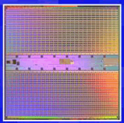
DRAM effectively utilizes one transistor per cell, allowing high densities but unfortunately operating at low speeds. SRAM utilizes six transistors per cell in a flip flop configuration, lowing density but allowing operation at several GHz. Below, Intel demonstrates a 110mm2 SRAM module with a 70Mbit capacity (over 500 million transistors). This is less than a modern BGA module can handle, but consider the SRAM module can operate several GHz faster than any DRAM module with ease.
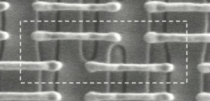
You can see an actual SRAM cell in the image below. The white dash outlines a cell with an area about 0.57um2.
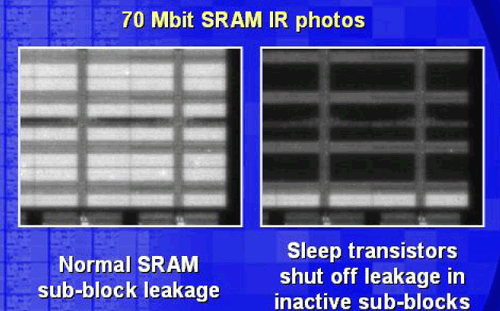
Simply designing more and more transistors on a chip does not make sense if thermal issues bog down the true capabilities of the processor. We spotted one new technology that did not receive a lot of attention during the presentations; the introduction of sleep transitors. Sleep transistors act as miniature controllers to an SRAM bank, throttling power during operating to reduce leakage. The sleep transistors themselves do not sleep, but rather the transistors they control do.
Further advances at Intel, like trigate transistors will essentially place transistor interconnects on a 3D grid instead of a 2D one - allowing for much higher densities without revamping lithography or gate size.
Intel already uses low-k dielectrics between their metal layers to reduce capacitance They use a Carbon Doped Oxide (CDO) for this, though they weren't specific about what oxide they are using for this. This will continue into 65nm, and strained silicon will see some slight revisions as well. Currently their silicon germanium (PMOS) and nickel silicide (NMOS) strained silicon gives about a 20% average improvement in transistor drive current, but Enhanced Strained Silicon (as they are calling it) promises a 30% average improvement.
At this point in time, Intel did not discuss exactly what makes their next step in strained silicon "enhanced", but they were fairly tight lipped about their original implementation before it hit the market.


21 Comments
View All Comments
mikecel79 - Thursday, September 9, 2004 - link
Great article on Intel's technology but why nothing about the dual core P4 they showed running on a 915 board yesterday?From the ZDnet article at http://zdnet.com.com/2100-1103_2-5356703.html
"Like the current Pentium 4, Intel's dual-core desktop chip is built on the NetBurst architecture and fits into motherboards using Intel's 915 Grantsdale chipset. But Siu declined to provide many details on the dual-core demonstration chip, which he described as an engineering prototype.
"It is real silicon running on a standard 915 platform," Siu said. He wouldn't comment on whether it has the 64-bit memory extension technology, called EM64T."