Intel 65nm and Beyond (or Below): IDF Day 2 Coverage
by Kristopher Kubicki on September 9, 2004 9:26 AM EST- Posted in
- Trade Shows
Silicon and Transistor Technology
Advances in lithography technology have only been half of the battle in fulfilling Moore's law. In fact, silicon and transistor technology itself has undergone radical changes in the last couple years (particularly with technology like strained silicon). Putting more transistors on a processor recently has had more to do with increasing cache size rather than increasing logic on the CPU. Advances in lithography and gate technology dramatically increase our density of other components such as SRAM - the building blocks of cache memory.
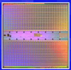
DRAM effectively utilizes one transistor per cell, allowing high densities but unfortunately operating at low speeds. SRAM utilizes six transistors per cell in a flip flop configuration, lowing density but allowing operation at several GHz. Below, Intel demonstrates a 110mm2 SRAM module with a 70Mbit capacity (over 500 million transistors). This is less than a modern BGA module can handle, but consider the SRAM module can operate several GHz faster than any DRAM module with ease.
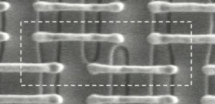
You can see an actual SRAM cell in the image below. The white dash outlines a cell with an area about 0.57um2.
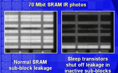
Simply designing more and more transistors on a chip does not make sense if thermal issues bog down the true capabilities of the processor. We spotted one new technology that did not receive a lot of attention during the presentations; the introduction of sleep transitors. Sleep transistors act as miniature controllers to an SRAM bank, throttling power during operating to reduce leakage. The sleep transistors themselves do not sleep, but rather the transistors they control do.
Further advances at Intel, like trigate transistors will essentially place transistor interconnects on a 3D grid instead of a 2D one - allowing for much higher densities without revamping lithography or gate size.
Intel already uses low-k dielectrics between their metal layers to reduce capacitance They use a Carbon Doped Oxide (CDO) for this, though they weren't specific about what oxide they are using for this. This will continue into 65nm, and strained silicon will see some slight revisions as well. Currently their silicon germanium (PMOS) and nickel silicide (NMOS) strained silicon gives about a 20% average improvement in transistor drive current, but Enhanced Strained Silicon (as they are calling it) promises a 30% average improvement.
At this point in time, Intel did not discuss exactly what makes their next step in strained silicon "enhanced", but they were fairly tight lipped about their original implementation before it hit the market.


21 Comments
View All Comments
RyanVM - Thursday, September 9, 2004 - link
I'm trying to figure out if you guys are using "Itanimum" because you're trying to be witty or just don't know that its name is "Itanium". I think my sarcasm meter might be broken.mrmorris - Thursday, September 9, 2004 - link
Interesting article, looking forward to getting "the big picture" when Intel competite technology is included (AMD).PrinceGaz - Thursday, September 9, 2004 - link
1T-SRAM is basically DRAM with a built in controller that handles all the refreshing etc, so it can be used in a similar way to SRAM.Because it uses DRAM technology, its nowhere near as fast as true SRAM and therefore unsuitable for use as cache memory.
Skykat - Thursday, September 9, 2004 - link
As I recall, the Nintendo Gamecube uses 1T-SRAM (1 transistor). Whatever happened to this technology? It would seem a lot more efficient than 6 Transistor SRAM. I think the Gamecube processor was manufactured by IBM though...ncage - Thursday, September 9, 2004 - link
#5 speed is NOT the ideal thing for what itanimum was made for. Itanimum is made for high end servers where caching is just as important as speed. Think of the high end scientific apps where the majority of the work is swapping data back and forth from ram to peform calculations on. Ya they could speed up the cpu but it would be cache starved and would be ide wile it was waiting to fetch data from main memory into cache/registers. Lots of cache is also ideal for large database appliations. One thing i am suprised is intel has not decided to go with an on die memory controller like AMD.mkruer - Thursday, September 9, 2004 - link
When I said double up on the logic I meant parallel processing, not making the logic more complex.mkruer - Thursday, September 9, 2004 - link
I will not say that I am disappointed, but I think I could sum this article up much faster, Intel has Awesome FAB capabilities, but too bad their chip designs are not the greatest. One day Intel might lean that instead of throwing huge amounts of cache to get everything to work faster, to double up on the logic. Just imagine if the Itanimum was cache efficient, with the amount of chip real-estate they could save they could easily double the core logic, and get a true boot in performance.nourdmrolNMT1 - Thursday, September 9, 2004 - link
i agree with number 3.MIKE
CrimsonDeath - Thursday, September 9, 2004 - link
Wow i feel really stupid right now...Johnmcl7 - Thursday, September 9, 2004 - link
Yeah, I fully agree I was a little disappointed the article seemed to end rather abruptly, however it was an interesting read otherwise.Also, shouldn't it be 'extensions of Moore's Law' rather than 'extentions'?
John