The NVIDIA Turing GPU Architecture Deep Dive: Prelude to GeForce RTX
by Nate Oh on September 14, 2018 12:30 PM ESTThe Turing Architecture: Volta in Spirit
Diving straight into the microarchitecture, the new Turing SM looks very different to the Pascal SM, but those who’ve been keeping track of Volta will notice a lot of similarities to the NVIDIA’s more recent microarchitecture. In fact, on a high-level, the Turing SM is fundamentally the same, with the notable exception of a new IP block: the RT Core. Putting the RT Cores and Tensor Cores aside for now, the most drastic changes from Pascal are same ones that differentiated Volta from Pascal. Turing’s advanced shading features are also in the same bucket in needing explicit developer support.
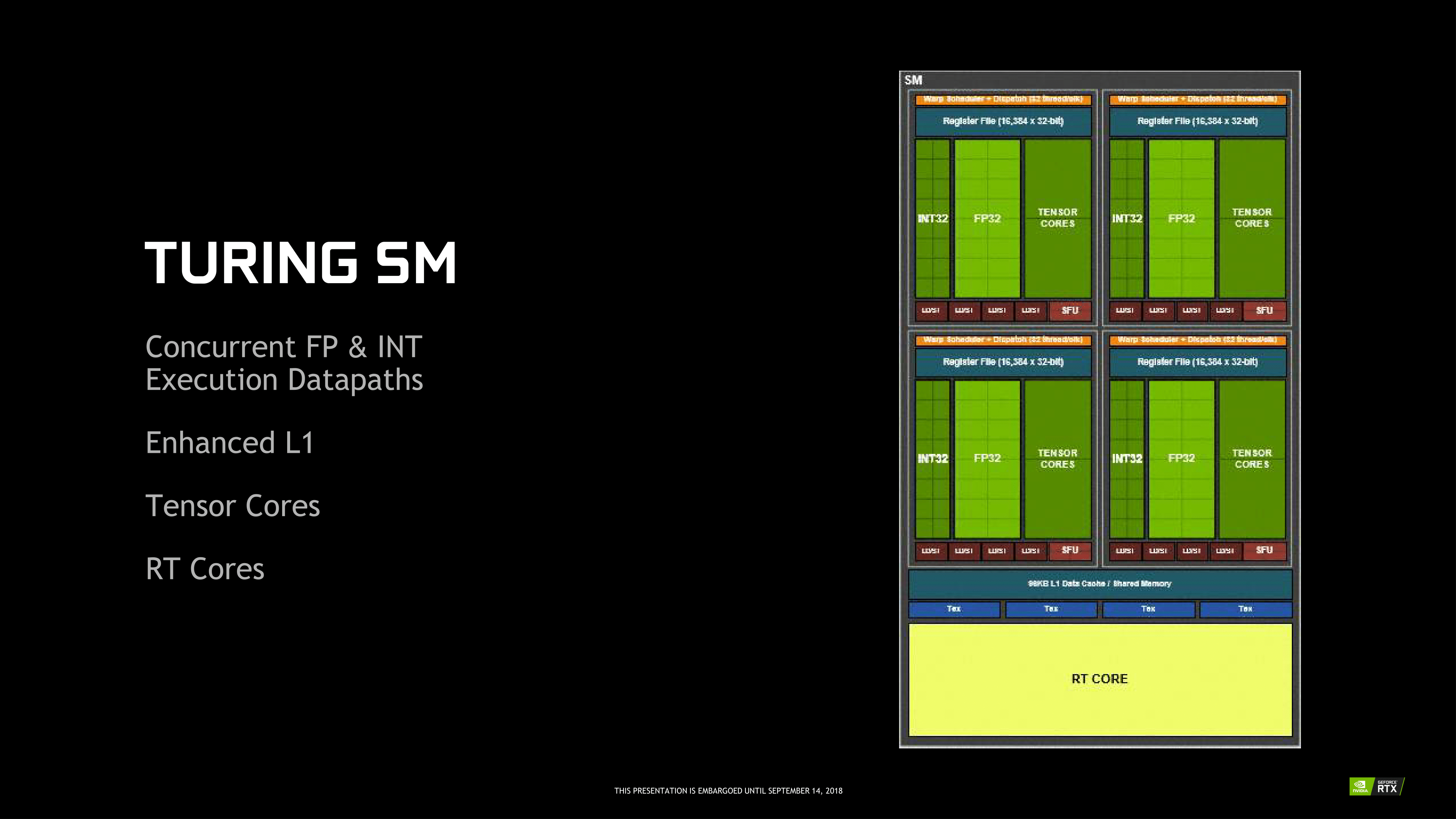
Like Volta, the Turing SM is partitioned into 4 sub-cores (or processing blocks) with each sub-core having a single warp scheduler and dispatch unit, as opposed Pascal’s 2 partition setup with two dispatch ports per sub-core warp scheduler. There are some fairly major implications with change, and broadly-speaking this means that Volta/Turing loses the capability to issue a second, non-dependent instruction from a thread for a single clock cycle. Turing is presumably identical to Volta performing instructions over two cycles but with schedulers that can issue an independent instruction every cycle, so ultimately Turing can maintain 2-way instruction level parallelism (ILP) this way, while still having twice the amount of schedulers over Pascal.
Like we saw in Volta, these changes go hand-in-hand with the new scheduling/execution model with independent thread scheduling that Turing also has, though differences were not disclosed at this time. Rather than per-warp like Pascal, Volta and Turing have per-thread scheduling resources, with a program counter and stack per-thread to track thread state, as well as a convergence optimizer to intelligently group active same-warp threads together into SIMT units. So all threads are equally concurrent, regardless of warp, and can yield and reconverge.

In terms of the CUDA cores and ALUs, the Turing sub-core has 16 INT32 cores, 16 FP32 cores, and 2 Tensor Cores, the same setup as the Volta sub-core. With the split INT/FP datapath model like Volta, Turing can also concurrently execute FP and INT instructions, which as we will see, is much more relevant with the RT cores involved. Where Turing differs is in lacking Volta’s full complement of FP64 cores, instead having a token amount (2 per SM) for compatibility reasons and resulting in FP64 throughput being 1/32 the TFLOP rate of FP32. Maimed FP64 is standard for NVIDIA’s consumer GPUs, but what has not been standard until now is Turing’s full 2x FP16 throughput, which was available in GP100 but was crippled in the other Pascal GPUs.
While these details may be more on the technical side of things, in Volta this design seemed inextricably linked to maximizing the most amount of performance from tensor cores, but minimizing disrupting parallelism or coordination with other compute workloads. The same is most likely true with Turing’s 2nd generation tensor cores and RT cores, where 4 independently scheduled sub-cores and granular thread manipulation would be very useful in extracting the most performance out of mixed gaming-oriented workloads, where rendering a single frame would be pulling in multiple blocks of the GPU to work in conjunction. This is actually a concept that circumscribes the RTX-OPS metric, and we will revisit that in depth later.
Memory-wise, every sub-core now has an L0 instruction cache like Volta, with identically sized 64 KB register file. In Volta, this was important in reducing latency when the tensor cores were in play, and in Turing this likely benefits RT cores similarly, which we will discuss in a later section. Otherwise, the Turing SM also has 4 load/store units per sub-core, down from 8 in Volta, but still maintains 4 texture units.
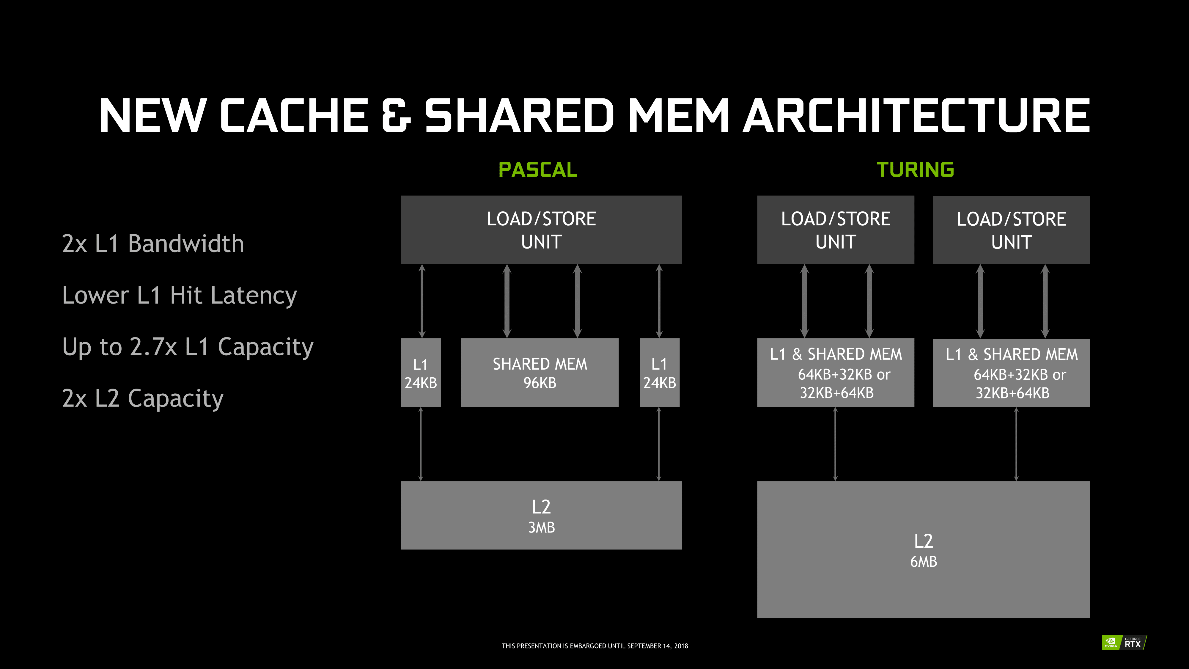
Further up the memory hierarchy is the new L1 data cache and Shared Memory (SMEM) that has been revamped and unified into a single partitionable memory block, another Volta innovation. For Turing, this is looking to be a combined 96 KB L1/SMEM, which traditional graphics workloads divide as 64KB for dedicated graphics shader RAM and as 32 KB for texture cache and register file spill area. Meanwhile, compute workloads can partition the L1/SMEM with up to 64 KB as L1 with the remaining 32 KB as SMEM, or vice versa. For Volta, SMEM can be configured up to 96 KB.
Though many of these details are only of value to developers, there are several important points to make here. One is simply how similar Turing and Volta are, as opposed to ; after all, they are in the same generational compute family. Another is how compute-oriented Volta – and by extension, Turing – are, and the fact that this is being brought to consumers as part of NVIDIA’s proclaimed ‘future of gaming.’ Part of that is, of course, permitting fast FP16 in potential gaming workloads, but Turing goes far beyond that. At the low level, Turing is less about maximizing traditional gaming, and more about maximizing gaming with special technologies such as real-time raytracing.
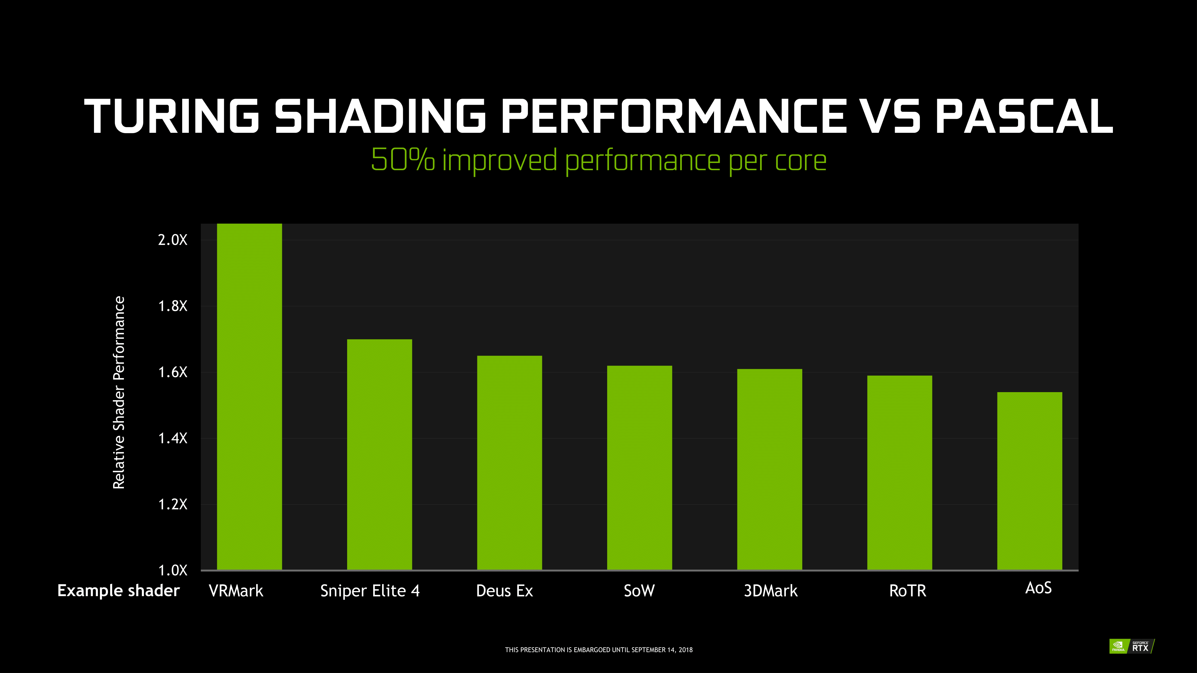
For their part, NVIDIA points to Turing’s leap in performance from Pascal, from memory hierarchy bandwidth uplifts to 50% more shader performance per core, but unfortunately for today we can’t connect this with any real world data or performance. With concurrent FP/INT execution in gaming, the company is keen to point out that around 36 INT instructions could be freed up by moving to its own pipe, which nevertheless doesn’t describe Turing performance, only the applicability of its concurrent execution feature in games.
It becomes a bit of a complex scenario, as we know that Volta already improved on Pascal in these aspects with concurrent execution, a brand new ISA, and reworked SM. And it doesn’t seem to involve architectural changes for significant clockspeed enhancements a la Pascal from Maxwell, though of course on the process side the 12nm FFN is a factor. So it comes down to special gaming workloads and real-world performance. The latter is not available today, but the former is so important to Turing that it merited dropping ‘GTX’ for ‘RTX’. And of those special workloads, real-time raytracing and RT cores take center stage.


111 Comments
View All Comments
Tamz_msc - Saturday, September 15, 2018 - link
"Besides, what you said isn't true even limiting the discussion to what was covered in this article. The Turing Tensor cores allow for a greater range of precisions."You mean lower precision, right? INT8 and INT4 are lower range. From a higher-level view Volta is very similar to Turing, just like the OP described.
Yojimbo - Saturday, September 15, 2018 - link
"greater range of precisions"INT8, INT4, FP16, etc., are precisions. The range of precisions an architecture can handle is the set of all precisions it can handle. Turing Tensor Cores can handle INT4, INT8, and FP16, whereas Volta Tensor Cores can handle FP16. So Turing can handle a greater range of precisions.
Bulat Ziganshin - Friday, September 14, 2018 - link
I would pray for 2060 w/o all this RT/FP16 stuffSpunjji - Monday, September 17, 2018 - link
Seems likely given how nutso these die sizes are. I expect we won't see it until after Pascal inventory is cleared, though.Da W - Friday, September 14, 2018 - link
Well still playing on my 3-screen Haswell + GTX780 rig, and being pretty satisfied of it, i'll probably just get a cheap GTX 1070 or 1080 for my new Ryzen rig and wait if ray tracing really gets adopted in 1 or 2 years. Seems to me lots of transistors invested for not many games. If history told us anything, it's not because a technology is great that it will get adopted, especially if it asks LOADS more developper time for the game companies.Not sure AMD won't come up with something either down the line. They've been given for dead for over 2 decades, guess where they are now!
Holliday75 - Monday, September 17, 2018 - link
I am waiting as well. This is the first attempt to change the game. Next gen or two is where it will be fined tuned and worth purchasing. This feels like a 4k TV purchase. Waste of money.abufrejoval - Friday, September 14, 2018 - link
I wonder how much Turing is about staking out territorial claims vs. dark silicon also coming to GPUs...Obviously Nvidia wants to protect its CUDA machine learning and HPC empire against custom ASIC competitors which finally also include Intel with their Configurable Spatial Accellerator, as well as Cambricon, Google's TPU ASICs and far too many others for comfort.
But while many seem to bemoan that tensor core or rasterizing real-estate is a waste for gaming and just about raising the purchase prices with overhyped features nobody needs, I wonder if apart from the partial truth in that the other motivating driver is simply that the inability to translate additional transistors into additional performance as additional bandwidth requires step changes in GDDR6 lanes (with unshrinkable pad areas and amplifiers) and hits foundry reticle sizes.
So they had transistors left over (wonder where those came from without a die shrink: I/O voltage reduction, layout optimizations, really bigger chips?), that could not be turned into direct DX1x performance gains due to bandwidth and TDP constraints and going to a richer functional base with Tensor Cores and raytrace assists would eat alternate bandwidth or TDP budgets, not additional ones.
Any truth in those assumptions?
abufrejoval - Friday, September 14, 2018 - link
ok, much bigger chips...And no rip-off: They are worth what they are charging if only for the inference accelleration.
Yojimbo - Saturday, September 15, 2018 - link
I am not convinced the Tensor Cores take up a lot of real estate. And they are tightly integrated into NVIDIA's SMs. Designing two SMs, one with Tensor Cores and one without Tensor Cores would be a lot more expensive than leaving them in. Plus, NVIDIA sees deep learning as important for gaming.Your argument about FLOPS per bandwidth does have validity. It's just that neither Tensor Cores nor RT cores were just thrown in there because they had transistors left over. Look at the die sizes of these new GPUs compared to Pascal GPUs. If they built a smaller chip that performed the same in legacy games then they could sell them more cheaply, and so sell more of them, while making the same profit on each one. That would mean higher margins and greater profits.
The RTX and Tensor Cores are a strategic initiative. I think in making the decision to include them NVIDIA judged that those two technologies would have a positive impact on the future of gaming. The reason they made that judgment may include the dwindling FLOPS/memory bandwidth trend.
bernstein - Friday, September 14, 2018 - link
really interesting time in gpu's right now... remember a decade ago when intel teased a x86-gpu that promised to do real-time raytracing?yet turing may turn out to provide an abysmal price/perf ratio.
- about half the transistors will only be used in a few upcoming games, they could be used to possibly double performance in rasterization-only games (7nm amd navi anyone?)
- but if (hybrid-)raytracing takes off quickly, turing will be crushed by 7nm gpu's dedicating way more transistors to the task, as it's performance is still skewed heavily towards rasterization
- ai inferencing seems like a safe bet, again i'd wager that DLSS will only ever work with the vast minority of games released each day on steam, so it's usefulness will depends on whether developers make other use of the available silicon... (better AI opponents anyone?)