Arm's Cortex-A76 CPU Unveiled: Taking Aim at the Top for 7nm
by Andrei Frumusanu on May 31, 2018 3:01 PM EST- Posted in
- CPUs
- Arm
- Smartphones
- Mobile
- SoCs
- Cortex-A76
Cortex A76 µarch - Backend
Switching to the back-end of the core we have a look at the execution core.

The integer core contains 6 issue queues and execution ports (4 depicted in the slide plus 2 load/store pipelines). There are 3 integer execution pipelines – two ALUs capable of simple arithmetic operations and a complex pipeline handling also multiplication, division and CRC ops. The three integer pipelines are served by 16 deep issue queues. The same size issue queue can also be found serving the single branch execution port.
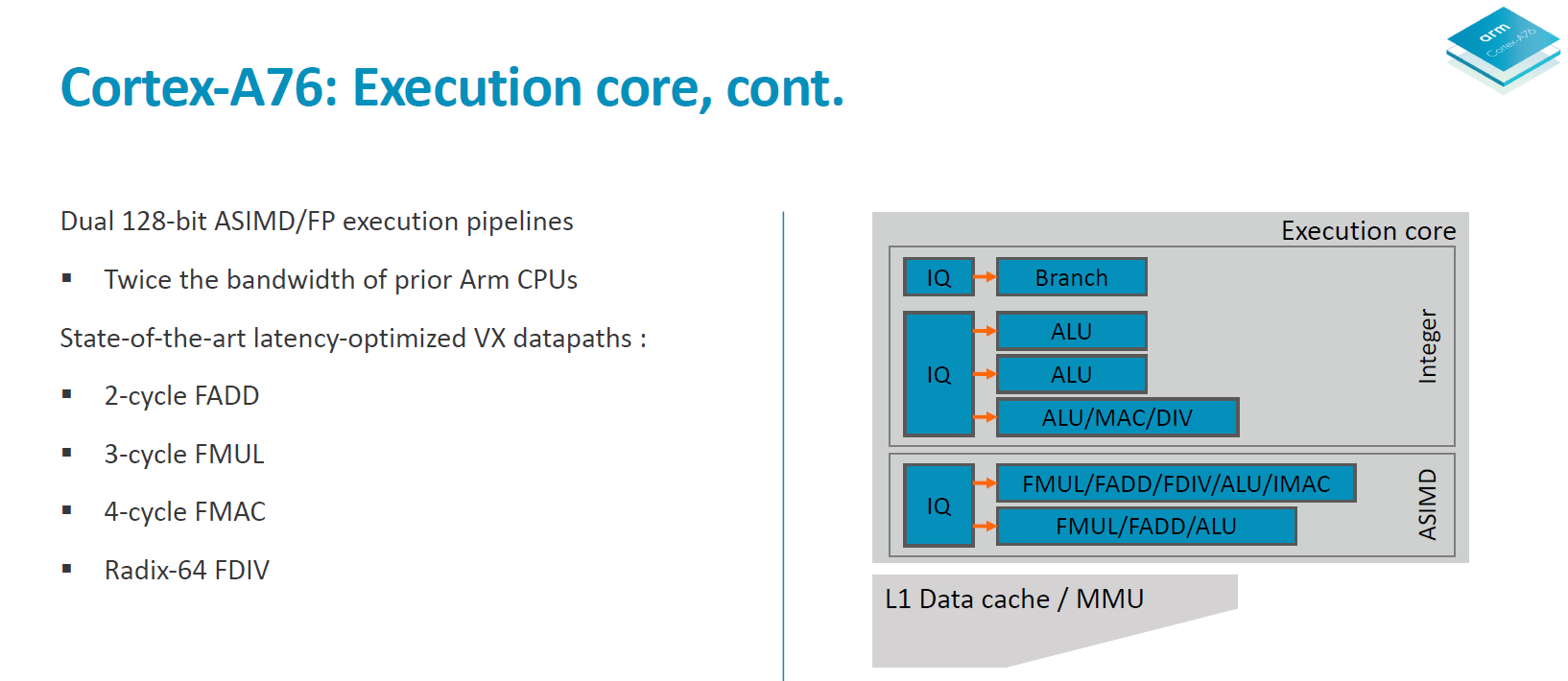
Two load/store units are the remaining ports of the integer core and are each served by two 12 deep issue queues. The issue queue stages are 3 cycles deep and while I mentioned that the rename/dispatch is 1 stage deep, the dispatch stage actually overlaps with the first cycle of the issue queues stages.
The ASIMD/floating point core contains two pipelines which are served by two 16-deep issue queues.
When it comes to the backend of a CPU core the two most important metrics are instruction throughput and latency. Where the A76 in particular improves a lot is in terms of instruction latency as it’s able to shave off cycles on very important instructions.
To better overview the improvements I created a table with the most common instruction types. The execution throughput and latencies presented here are for AArch64 instructions and if not otherwise noted represent operations on 64-bit data for integer and 64bit (double precision) FP.
| Backend Execution Throughput and Latency | ||||||
| Cortex-A75 | Cortex-A76 | Exynos-M3 | ||||
| Exec | Lat | Exec | Lat | Exec | Lat | |
| Integer Arithmetic (Add, sub) | 2 | 1 | 3 | 1 | 4 | 1 |
| Integer Multiply 32b | 1 | 3 | 1 | 2 | 2 | 3 |
| Integer Multiply 64b | 1 | 3 | 1 | 2 | 1 (2x 0.5) |
4 |
| Integer Multiply Accumulate | 1 | 3 | 1 | 2 | 1 | 3 |
| Integer Division 32b | 0.25 | 12 | 0.2 | < 12 | 1/12 - 1 | < 12 |
| Integer Division 64b | 0.25 | 12 | 0.2 | < 12 | 1/21 - 1 | < 21 |
| Move (Mov) | 2 | 1 | 3 | 1 | 3 | 1 |
| Shift ops (Lsl) | 2 | 1 | 3 | 1 | 3 | 1 |
| Load instructions | 2 | 4 | 2 | 4 | 2 | 4 |
| Store instructions | 2 | 1 | 2 | 1 | 1 | 1 |
| FP Arithmetic | 2 | 3 | 2 | 2 | 3 | 2 |
| FP Multiply | 2 | 3 | 2 | 3 | 3 | 4 |
| FP Multiply Accumulate | 2 | 5 | 2 | 4 | 3 | 4 |
| FP Division (S-form) | 0.2-0.33 | 6-10 | 0.66 | 7 | >0.16 (2x 1+/12) |
12 |
| FP Load | 2 | 5 | 2 | 5 | 2 | 5 |
| FP Store | 2 | 1-N | 2 | 2 | 2 | 1 |
| ASIMD Arithmetic | 2 | 3 | 2 | 2 | 3 | 1 |
| ASIMD Multiply | 1 | 4 | 1 | 4 | 1 | 3 |
| ASIMD Multiply Accumulate | 1 | 4 | 1 | 4 | 1 | 3 |
| ASIMD FP Arithmetic | 2 | 3 | 2 | 2 | 3 | 2 |
| ASIMD FP Multiply | 2 | 3 | 2 | 3 | 1 | 3 |
| ASIMD FP Chained MAC (VMLA) | 2 | 6 | 2 | 5 | 3 | 5 |
| ASIMD FP Fused MAC (VFMA) | 2 | 5 | 2 | 4 | 3 | 4 |
On the integer operations side the A76 improves the multiplication and multiply accumulate latencies from 3 cycles down to 2 cycles, with the throughput remaining the same when compared to the A75. Obviously because the A76 has 3 integer pipelines simple arithmetic operations see a 50% increase in throughput versus the A75’s 2 pipelines.
The much larger and important improvements can be found in the “VX” (vector execution) pipelines which are in charge of FP and ASIMD operations. Arm calls the new pipeline a “state-of-the-art” design and this is finally the result that’s been hyped up for several years now.
Floating point arithmetic operations have been reduced in latency from 3 cycles down to 2 cycles, and multiply accumulate has also shaved off a cycle from 5 cycles down to 4.
What Arm means by the “Dual 128bit ASIMD” with doubled execution bandwidth is that for the A75 and prior only one of the vector pipelines was capable of 128bit while the other one was still 64-bit. For the A76 both vector pipelines are 128-bit now so quad-precision operations see a doubling of the execution throughput.
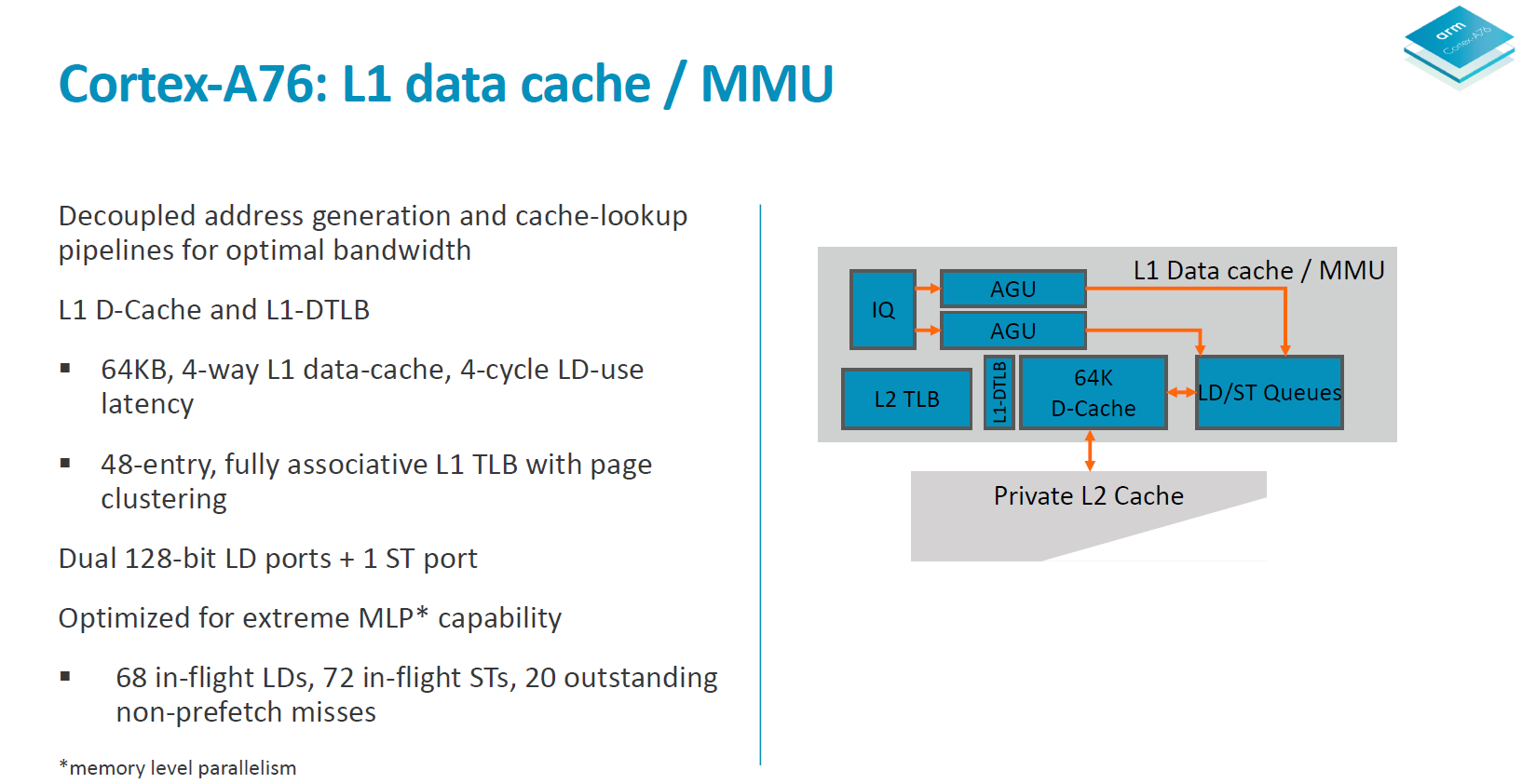
Moving onto more details of the data handling side, we see the again the two load/store pipelines which was something first implemented on the A73 and A75. Although depicted as one issue queue in the slide, the LD/S pipelines each have their own queues at 16 entries deep.
The data cache is fixed at 64KB and is 4-way associative. Load latency remains at 4 cycles. The DTLBs run a separate pipeline as tag and data lookup. Arm’s goals here is aiming for maximum MLP/ memory level parallelism to be able to feed the core.
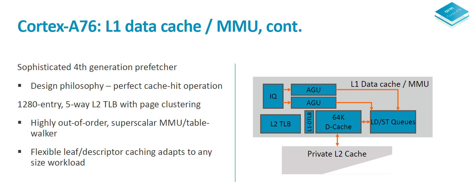
In a perfect machine everything would be already located in the caches, so it’s important to have very robust prefetching capabilities. On the A76 we see a new 4th generation prefetchers introduced to get nearer to this goal of perfect cache-hit operation. In all the A76 has 4 different prefetching engines running in parallel looking at various data patterns and loading data into the caches.
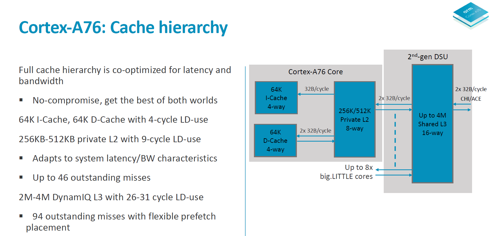
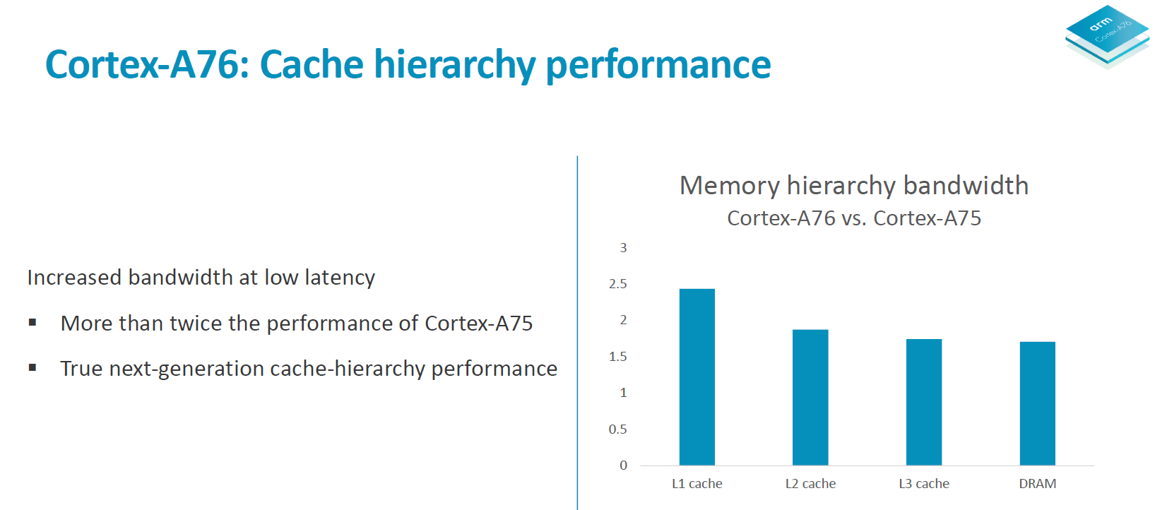
In terms of the A76 cache hierarchy Arm is said to have made no compromises and got the best of both worlds in terms of bandwidth and latency. The 64KB L1 instruction cache reads up to 32B/cycle and the same bandwidth applies to the L1 data cache in both directions. The L1 is a writeback cache. The L2 cache is configurable in 256 or 512KB sizes and is D-side inclusive with the same 2x 32B/cycle write and read interfaces up to the exclusive L3 cache in the 2nd generation DSU.
Overall the microarchitectural improvements on the core are said to improve memory bandwidth to DRAM by up to 90% in microbenchmarks.
All in all the microarchitecture of the A76 could be summed up in a few focus design points: Maximise memory performance throughout the core by looking at every single cycle. During the design phase the engineers were looking at feature changes with a sensitivity of up to 0.25% in performance or power – if that metric was fulfilled then it was deemed to be a worthwhile change in the core. Small percentages then in turn add up to create significant figures in the end product.
The focus on bandwidth on latency is said to have been extreme, and Arm was very adamant in re-iterating that to be able to take full advantage of the microarchitecture that vendors need to implement an equally capable memory subsystem on the SoC to see full advantages. A figure that was put out there was 0.25% of performance per nanosecond of latency to main memory. As we’ve seen in the Snapdragon 845 one of the reasons the SoC didn’t quite reach Arm’s projected performance metrics was the degraded memory latency figures which might have been introduced by the L4 system cache in the SoC. In the future vendors will need to focus more on providing latency sensitive memory subsystems as otherwise they’ll be letting free performance and power on the table with differences that could amount to basically a generational difference in CPU IP.


123 Comments
View All Comments
vladx - Friday, June 1, 2018 - link
That's weird, in most speed tests I've seen Android flagships beat iPhones in all but graphics-intensive apps like games and video editing.varase - Saturday, June 2, 2018 - link
Those tests are usually serially launching a bunch of apps, then round-robining.It's probably more a demonstration that Android phones have more RAM.
StrangerGuy - Sunday, June 3, 2018 - link
Yup, that totally has to do with hardware and not thing to do with UI optimizations and design choices = Apple sux lololBut hey, somebody in this world needs to get their daily dose of retarded Youtube clickbait shit videos. Bonus originality points when it's Apple-hating.
jospoortvliet - Wednesday, June 6, 2018 - link
Yeah, app developers make sure to keep the Android versions lighter to not let performance completely fall apart on all the many cheap 8x a53 SOC's out there... fi d a real equivalent app that does heavy stuff like render a large pdf or generate video's out of a bunch of pics and videos. I mean, really the same. Not sure if faster CPU and storage will not make a huge diff then...B3an - Thursday, May 31, 2018 - link
Do Anandtech writers know the meaning of the word "several"? I keep seeing it said on here, when you actually mean a "couple" or a "few" because you mean 2 or 3.StormyParis - Friday, June 1, 2018 - link
"several" means "more than one" so I'm not sure who's having a vocabulary issue. Or rather, I am.nico_mach - Friday, June 1, 2018 - link
In American English, it's coloquially taken as meaning more than a few (sounds like seven and his progression is correct, couple<few<several). But it's not universally understood that way. Several is perfectly understandable imo.If you want to quibble, the phrase 'my projects' in the third to last paragraph should be 'my projections'.
Gunbuster - Thursday, May 31, 2018 - link
Someone forget to update the PowerPoint deck full of "Laptop class performance" after the big nothing burger that is win 10 on ARM?nico_mach - Friday, June 1, 2018 - link
That was such a disappointing set of products. Just the price of them for the performance and spec.lilmoe - Thursday, May 31, 2018 - link
Nope. Still don't agree that efficiency at max clocks is indicator of anything in a smartphone form factor. Total power draw per worked is where it's at.This announcement shouldn't be comparable with the current 9810. I don't believe the a76 would fair well on 10nm, and definitely not in a quad core - high cache configuration. Samsung rushed the design; neither the OS/firmware nor the process were ready for that chip, but it still was competitive, despite not being to my liking. It would have kicked butt running windows on arm though.
The a76 and a12 at 7nm will be competing against the m4 at 7nm EUV. I don't want to get ahead of myself, but I have my money on Samsung. Here's to a GS10 released in one SoC configuration without holding any of its features or performance back.