Radeon RX Vega Unveiled: AMD Announces $499 RX Vega 64 & $399 RX Vega 56, Launching August 14th
by Ryan Smith on July 30, 2017 10:30 PM ESTFeatures & the Future Launch
Last but not least, along with today’s card announcements, AMD has also lifted the embargos on the architectural elements of the Vega 10 GPU. While there are no new architecture features to discuss – it turns out AMD was rather thorough with their preview at the start of this year – there’s still quite a bit in the way of details to dig into here. In fact it's more than I can hope to cover in a single day, let alone the few hours I’m getting to write this article ahead of AMD’s embargo. So I want to hit the highlights.
First and foremost, AMD has clarified that they do not consider Vega 10 to be a high performance computing (HPC) chip, unlike Hawaii. In particular, Vega 10’s native FP64 rate is just 1/16, like AMD’s other consumer chips. And the chip, while supporting HBM2’s native ECC mode, doesn’t have ECC on its internal pathways. This doesn’t mean that the chip can’t be placed in a server – its FP16 and INT16/INT8 performance is the cornerstone of its existence as part of the Radeon Instinct family. But that’s still a different market than traditional HPC. When we might see another HPC chip from AMD is anyone’s guess at this moment.
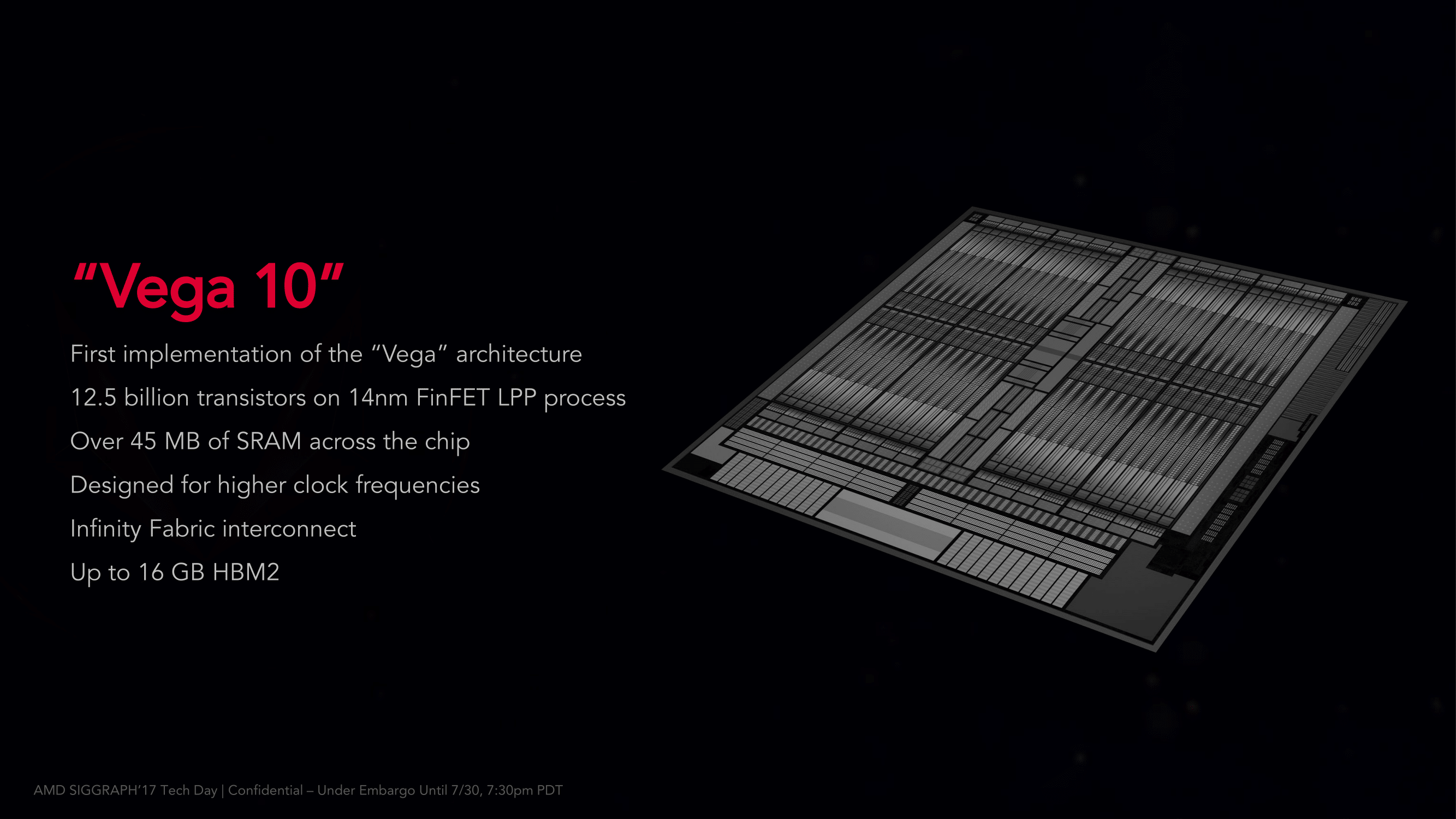
Second of all, we have a formal die size and transistor count for Vega 10. The GPU is officially 486mm2, containing 12.5B transistors therein. That amounts to 3.9B more transistors than Fiji – an especially apt comparison since Fiji is also a 64 CU/64 ROP card – all the while being 112mm2 smaller than Fiji (despite the higher transistor count) thanks to the higher density of GloFo’s 14nm LPP process, which AMD is using to fab the chip.
Talking to AMD’s engineers, what especially surprised me is where the bulk of those transistors went; the single largest consumer of the additional 3.9B transistors was spent on designing the chip to clock much higher than Fiji. Vega 10 can reach 1.7GHz, whereas Fiji couldn’t do much more than 1.05GHz. Additional transistors are needed to add pipeline stages at various points or build in latency hiding mechanisms, as electrons can only move so far on a single clock cycle; this is something we’ve seen in NVIDIA’s Pascal, not to mention countless CPU designs. Still, what it means is that those 3.9B transistors are serving a very important performance purpose: allowing AMD to clock the card high enough to see significant performance gains over Fiji.
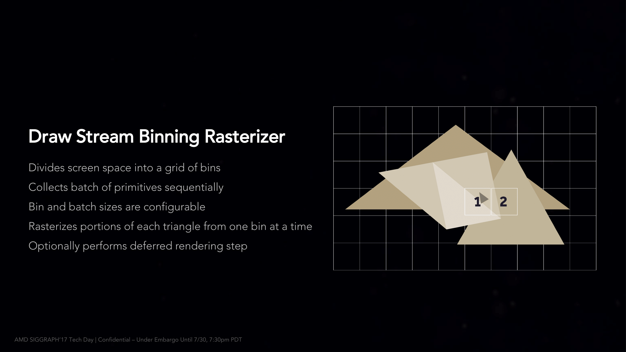
Speaking of Fiji, there’s been some question over whether the already shipping Vega FE cards had AMD’s Draw Steam Binning Rasterizer enabled, which is one of the Vega architecture’s new features. The short answer is that no, the DSBR is not enabled in Vega FE’s current drivers. Whereas we have been told to expect it with the RX Vega launch. AMD is being careful not to make too many promises here – the performance and power impact of the DSBR vary wildly with the software used – but it means that the RX Vega will have a bit more going on than the Vega FE at launch.
Fifth, AMD is tweaking their boost clock mechanism and how it's advertised. Up until now, the boost clock was the maximum clock a Radeon card would hit. e.g. a stock Fury X topped out at 1.05GHz, and a stock RX 580 at 1340MHz. Starting with Vega RX, however, the company's definition of the boost clock is changing to the highest clockspeed a card is guaranteed to hit, but not the absolute highest clockspeed it can hit under load. There are still some nuances I want to test once I have the hardware in-hand, but at first glance this sounds closer to NVIDIA's definition, where each and every card is allowed to reach its natural limit (for the stock voltage).
Finally, while AMD didn’t clarify exactly when this change was made, the company has tweaked their Freesync Low Framerate Compensation technology to work with monitors that have a 2x range between min and max refresh rates, as opposed to 2.5x at launch. I’m told that 2.5x (or better) is still the ideal range, but it now works at 2x. This is an important development because the Samsung CF791 monitor that AMD is discounting as part of the Radeon Pack bundles has a 48Hz to 100Hz range; so it wouldn’t have been LFC capable under the old LFC rules.
Overall AMD has given us a lot to chew on – and more that can be covered in a single afternoon – but we still haven’t seen the whole picture. Today’s announcement of the card specifications and prices sets a very important baseline for what we should expect on August 14th, but no hard performance numbers to judge the final product. As I said at the start of this article, AMD’s marketing has done a very good job keeping Vega in the public’s mind. And today’s announcement is the next phase of that plan. But the end is approaching, and RX Vega’s full launch is drawing near, so it will be very interesting to see how everything we’ve learned over the last several months translates into gaming performance, power efficiency, and where AMD’s new place shall be in the realm of high-end video cards.


162 Comments
View All Comments
fanofanand - Wednesday, August 2, 2017 - link
it just shows the rate of advancement has slowed.Dug - Monday, July 31, 2017 - link
I would of gladly bought this bundle if they offered the Samsung C32HG70.Which I find much more appealing for gaming than ultrawide.
eva02langley - Monday, July 31, 2017 - link
Never seen so much hate for a product not even released and benchmarked.I will wait for the review before judging anything. People to tend the effect of drivers and architectures. Nobody take into account HBM 2 and it could be way more important than what people believed.
Once again, I only see nVidia fanboys burning their banners and going to war.
Tewt - Monday, July 31, 2017 - link
Agree and only Nvidia can get away with a large TDP. Anytime AMD releases something, somehow its OMG lets fry some bacon, when Nvidia does it the response is puh-leez what's an extra $20 a year.Regardless, I'm very happy with my RX 470.
madwolfa - Monday, July 31, 2017 - link
And when was it, 2010? We're in 2017, dude. Can't release hot shit liek that in this day.JasonMZW20 - Monday, July 31, 2017 - link
It seems GCN's static partitioning of CUs/TMUs/ROPs will need to give way to something more efficient and dynamic; I think GCN 5 is the last of its line. However, Nvidia achieves relatively good TBP by offloading some functions to the CPU. The selling point looks good though, as it's so much lower. Overall total system draw may not be too dissimilar.Any new architecture will need to incorporate a very large L2 cache, not unlike Pascal, and even on the CPU front, Ryzen; the render back-ends on Vega are L2 clients now, but I don't have data on the size of L2 cache on Vega 10. That takes up precious die-space, so what will get the axe? Hardware scheduling? Perhaps nothing at all? Moving to 7nm will free up some of that burden. We already know that the not-too-distant future of GPUs is MCM (multi-chip modules), just like CPUs. It'll be interesting to see what solutions transpire when the time comes.
AMD targeted Vega 10 for 225w. That has ballooned to 295w (air) and 345w (water). So, I think GCN wasn't designed, at the very beginning, with high-clocks in mind. A whole new rethink will need to be done for Navi to take the fight to Nvidia's Volta and future architectures.
CiccioB - Monday, July 31, 2017 - link
The fact is that GCN is performing so poorly in gaming that AMD needs to clock it up a lot to get some decent performances for the used silicon. And that goes against thermal efficiency, of corse.Ananke - Monday, July 31, 2017 - link
AMD is using a ring topology, and NVidia was two-way bus, I think. AMD inherited that from co-work with IBM fifteen years ago, and from ATI acquisition. Essentially, AMD's architecture is more like a supercomputers type with ability to transfer large data blocks, and NVidia is relying on cheaper narrow bus with compression, decompression and data predictions, but can achieve higher clock speeds...AMD missed to take on board software developers, NVidia popularized CUDA meanwhile, although for heavy computations AMD would be probably better, hence the crypto- currency preference to run better on AMD since the days of bitcoin, SETI and so on.
Considering so many foreign investors with material influence, I don't think AMD stands a chance outside the consumer market - from defense security point is a no go. I wish them luck , and I buy AMD for my gaming hobby, but realistically, they are not part of the big technology scene anymore.
Oxford Guy - Monday, July 31, 2017 - link
"they are not part of the big technology scene anymore."Did you sleep and miss Ryzen, Thread Ripper, and Epyc?
Oxford Guy - Monday, July 31, 2017 - link
Vulkan, which appears to be mainly an offshoot of Mantle, also has finally given Linux the ability to fully compete with DirectX.