NVIDIA's Back with NV35 - GeForceFX 5900 Ultra
by Anand Lal Shimpi on May 12, 2003 8:53 AM EST- Posted in
- GPUs
Stage 5: Shading/Texturing
The shading/texturing stage is single handedly responsible for the most amount of confusion in the GPU world these days. Originally, before the advent of the programmable GPU (DX8/DX9 class hardware), this stage consisted of reading pixels, texturing them (through the use of register combiners) and either looping the process or passing them on to the next stage. In those days, it was very easy to define how many pixels you could send through this stage in a given clock and what the throughput of this stage would be.
As we've made it a point to mention, each individual stage of the graphics pipeline is actually composed of multiple individual pipeline stages, this shading/texturing stage is no different. Before the days of programmable GPUs, the number of pixels in/out of this stage was fairly fixed and thus the marketing folks started recognizing these pipelines as rendering pipelines in the graphics core. The more pixels you could pass through this stage in parallel, the more robust your hardware. It provided an excellent way of differentiating previous generation hardware from the current generation; we saw consumer graphics evolve from a single pixel pipe to two, to four and eventually to eight.
The other method for classification ended up being the number of textures these pipelines could apply to a pixel passing through them in a given clock. We saw designs that were able to apply one, two or three textures per pixel, per pipe, per clock and thus the marketing folks were once again able to come up with nice terms such as pixel and texel fill rate (a way of representing the number of textured pixels a GPU could produce). However, once programmable GPUs began surfacing, it became much more difficult to characterize hardware by the number of pixel pipelines that exist in the GPU. In order to understand why, we must understand exactly what a "pixel pipeline" is.
Like most parts of the GPU, these pixel pipelines are nothing more than collections of execution units - adders, multipliers, etc… that have a specific task. There are significantly more execution units in a GPU than there are in a CPU; for example, the Pentium 4 features 3 general purpose floating point units (FPUs), whereas the NV35 features a total of 32 FPUs in its shading/texturing stage alone. The difference between the two is that the NV35's FPUs are much more specialized than what you'd encounter in a general purpose CPU like the Pentium 4 or Athlon XP.
Since programmable GPUs are going to have to execute custom code in the form of shader programs as well as perform the usual texture-and-go functionality of the old days, it has become much more difficult for marketing folks to characterize exactly how many "pixel pipes" exist in modern GPUs.
The number of pixel pipes has always been related to the number of pixels you could spit out every clock cycle; now, with the introduction of fully programmable pipelines that number can vary rather significantly depending on what sort of operations are carried out through the pipe.
Think of these pixel rendering pipelines, not as independent pathways, but as a farm of execution resources that can be used in any way. There are a number of adders that can be used either in parallel, or in series, with the result of one being fed to the input of another. If we were to characterize the number of pipelines by the number of pixels we could send through there in parallel then we could end up with numbers as low as 2 or as high as 16.
What the marketing folks have done to help clear up the confusion is come up with a list of scenarios and the throughput of their GPUs in those scenarios; for example, the following chart from NVIDIA:
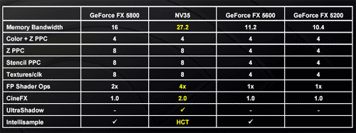
As you can see, there is sufficient hardware in the NV35 to guarantee a throughput of 8 pixels per clock in most scenarios, but in older games (e.g. single textured games) the GPU is only capable of delivering 4 pixels per clock. If you correctly pack the instructions that are dispatched to the execution units in this stage you can yield significantly more than 8 pixel shader operations per clock. For example, in NVIDIA's architecture a multiply/add can be done extremely fast and efficiently in these units, which would be one scenario in which you'd yield more than 8 pixel shader ops per clock.
It all depends on what sort of parallelism can be extracted from the instructions and data coming into this stage of the pipeline. Although not as extreme of a case (there isn't as much parallelism in desktop applications), CPUs enjoy the same difficulty of characterization. For example, the AMD Athlon XP has a total of 9 execution units, but on average the processor yields around 1 instruction per clock; the overall yield of the processor can vary so much depending on available memory bandwidth and the type of data it's working on among other things.
ATI's R3xx architecture differs from NVIDIA slightly in this respect, as they are able to output 8 pixels per clock in every one of the situations listed above. The advantage isn't huge as it is mostly limited to older games, but the difference does exist and is worth pointing out.


19 Comments
View All Comments
hivix - Wednesday, December 26, 2018 - link
hello this gonna works for you https://gamescraft.co/gamescraft-org-ml/seoshouts - Saturday, December 29, 2018 - link
Nvidia is the best graphic card i have used among.https://www.linkedin.com/company/orlando-seo-consu...
johncena2018 - Sunday, January 13, 2019 - link
https://freemusicallyfollowers.club/saber2 - Monday, February 25, 2019 - link
can I use it to Fortnite ? https://star2fut.fr/achat-v-bucks-fortnite-pas-che...don't sure
happywheelspace - Monday, June 3, 2019 - link
Great to know about this. Worth reading article, https://happywheelspace.com/yeeeeman - Tuesday, August 6, 2019 - link
Hi. Can you please update the graphs on these articles, since they don't show up anymore?spaces - Friday, February 28, 2020 - link
It's worth knowing it, thanks for sharing https://geometrydashspace.com/NewCM - Sunday, September 20, 2020 - link
So we can see here for soemthing important.https://enoot.eu/