Ten Year Anniversary of Core 2 Duo and Conroe: Moore’s Law is Dead, Long Live Moore’s Law
by Ian Cutress on July 27, 2016 10:30 AM EST- Posted in
- CPUs
- Intel
- Core 2 Duo
- Conroe
- ITRS
- Nostalgia
- Time To Upgrade
Core: Load Me Up
When discussing the size of the reorder buffer, I mentioned that for some ops relying on the data of others, the order in which they need to be processed has to remain consistent – the load for the second op has to follow the store from the first in order for the calculation to be correct. This works for data that is read from and written to the same location in the same data stream, however with other operations, the memory addresses for loads and stores are not known until they pass the address generation units (AGUs).
This makes reordering a problem at a high level. You ultimately do not want a memory location to be written and stored by two different operations at the same time, or for the same memory address to be used by different ops while one of those ops is sitting in the reorder queue. When a load micro-op enters the buffer, the memory addresses of previous stores are not known until they pass the AGUs. Note, that this applies to memory addresses in the caches as well as main memory. However, if one can speed up loads and load latency in the buffers, this typically has a positive impact in most software scenarios.
With Core, Intel introduced a ‘New Memory Disambiguation’. For lack of a better analogy, this means that the issue of loads preceding stores is given a ‘do it and we’ll clean up after’ approach. Intel stated at the time that the risk that a load will load a value out of an address that is being written to by a store that has yet to be finished is pretty small (1-2%), and the chance decreases with larger caches. So by allowing loads to go head of stores, this allows a speedup but there has to be a catch net for when it goes wrong. To avoid this, a predictor is used to help. The dynamic alias predictor tries to spot this issue. If it happens, the load will have to be repeated, with a penalty of about 20-cycles.
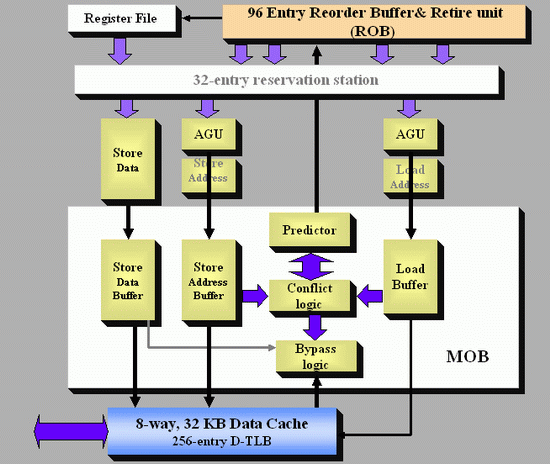
Unofficial AnandTech Diagram
The predictor gives permission for a load to move ahead of a store, and after execution the conflict logic scans the buffer in the Memory reOrder Buffer (MOB) to detect an issue. If it happens, then the load is reprocessed back up the chain. In the worst case scenario, this might reduce performance, but as Johan said back in 2006: ‘realistically it is four steps forward and one step back, resulting in a net performance boost’.
Using this memory disambiguation technique, Intel reported a 40% performance boost purely on allowing loads to be more flexible in a number of synthetic loads (or 10-20% in real world), along with L1 and L2 performance boosts. It is worth noting that this feature affects INT workloads more often than FP workloads, purely on the basis that FP workloads tend to be more ordered by default. This is why AMD’s K8 lost ground to Intel on INT workloads, despite having a lower latency memory system and more INT resources, but stayed on track with FP.
Core: No Hyper-Threading, No Integrated Memory Controller
In 2016, HT and an integrated memory controller (IMC) are now part of the fundamental x86 microarchitecture in the processors we can buy. It can be crazy to think that one of the most fundamental upticks in x86 performance in the last decade lacked these two features. At the time, Intel gave reasons for both.
Simultaneous Hyper-Threading, the act of having two threads funnel data through a single core, requires large buffers to cope with the potential doubling of data and arguably halves resources in the caches, producing more cache pressure. However, Intel gave different reasons at the time – while SMT gave a 40% performance boost, it was only seen as a positive by Intel in server applications. Intel said that SMT makes hotspots even hotter as well, meaning that consumer devices would become power hungry and hot without any reasonable performance improvement.
On the IMC, Intel stated at the time that they had two options: an IMC, or a larger L2 cache. Which one would be better is a matter for debate, but Intel in the end went with a 4 MB L2 cache. Such a cache uses less power than an IMC, and leaving the IMC on the chipset allows for a wider support range of memory types (in this case DDR2 for consumers and FB-DIMM for servers). However, having an IMC on die improves memory latency significantly, and Intel stated that techniques such as memory disambiguation and improved prefetch logic can soak up this disparity.
As we know know, on-die IMCs are the big thing.


158 Comments
View All Comments
Akrovah - Wednesday, July 27, 2016 - link
My old E6700 is still alive and kicking. I only just replaced it as my primary system when Devil's Canyon came along. Still use it for my four year old's "first computer."djayjp - Wednesday, July 27, 2016 - link
Not a particle physicist, nor electrical engineer, so just some pie in the sky wondering here, but wouldn't it be possible to build transistors using carbon nanotubes, or light itself (using nano sized mirrors/interferometers, like DLP) or even basing the transistor gates off of protons/sub atomic particles?michael2k - Wednesday, July 27, 2016 - link
I think a more interesting question is using glass as a substrate. Imagine printing nand, CPU, GPU, ram, and along the bezels of a smartphone.That reduces a phone to six components: a display, a transducer for sound, a mic, a battery, a radio, and a chassis, which would have all the antennas.
joex4444 - Wednesday, July 27, 2016 - link
Particle physicist here. Light has the tricky property that it travels at the speed of light so I can't imagine it working but perhaps I'm envisioning your concept differently than you are. For carbon nanotubes, you'll need a materials engineer or a condensed matter physicist.3DoubleD - Wednesday, July 27, 2016 - link
Materials/Semiconductor Physics Engineer here. The problem is not what we CAN do, the problem is what is economically possible at scale. For example, FinFETs were demonstrated at the turn of the century, but took all of those years to become (1) necessary - planar transistor were getting too leaky, and (2) possible to fabricate economically in large scales.Researchers have created smaller, faster transistors years ago, but it takes a lot of time and effort to develop the EUV or quadruple patterning technologies that enable these devices to be reliably and affordably manufactured.
So I think the problem in moving "beyond silicon" is not that we don't have alternatives, it is that we have many alternatives, we just don't know which will scale. It becomes less of a purely engineering problem and manufacturing business problem. When new technologies relied purely on the established silicon industry alone, you could reasonably extrapolate how much each new technology would cost as the nodes were scaled down. When we talk about using III-V FinFETs/ All Around Gates or graphene and carbon nanotubes, we don't really know how those things will scale with the existing processes as we move them from the laboratory to the manufacturing line.
I've been looking forward to this transition for years. People moan that it is the end of Moores Law, but that could be a good thing. Silicon is a great material for forming logic circuits for many reasons, but it also has many downsides. While silicon never reached 10 GHz (as Intel once predicted), other materials easily blow past 100 GHz transistor switching speeds. When the massive engines that work tirelessly to reduce our lithography nodes nm by nm are aimed at "the next big thing", we might be pleasantly surprised by a whole new paradigm of performance.
So what competes with modern day Si CMOS on speed, power usage, and cost? Nothing... yet!
djayjp - Thursday, July 28, 2016 - link
Yes, it's fascinating stuff. Thanks for reminding me about that. I recall now that I think it was graphene that enabled those insanely high switching speeds, due to its incredible conductivity/efficiency. Hopefully it can now be made economically feasible at some point! Imagine a the next GPU that is 10x smaller and operates at 100x the clock speed. A GTX 1080Ti x 1000! Finally we can do real time true global illumination ha....jeffry - Monday, August 1, 2016 - link
Thats a good point. Like, answering a question "are you willing to pay $800 for a new CPU to double the computers speed?" Most consumers say no. It all comes down to the mass market price.wumpus - Thursday, August 4, 2016 - link
From the birth of the Univac until 10 years ago, consumers consistently said YES! and plunked down their money. Doubling the (per thread) speed of a core2duo is going to cost more than $800. Also the cost of the RAM on servers is *WAY* more than $800, so you can expect if Intel could double the power of each core, they could crank prices up by at least $800 per core on Xeons. They can't, and neither can IBM or AMD.Jaybus - Thursday, July 28, 2016 - link
Sure, but that speed is dependent on the medium. There are some proposed optical transistors using electromagnetically induced transparency. Long way off. However, silicon photonics could change some things. Capacitance is the killer for electronic interconnects, whether chip-to-chip or on-chip bus. An optical interconnect could greatly increase bandwidth without increasing the chip's power dissipation. I think an electronic-photonic hybrid is more likely, since silicon photonics components can be made on a CMOS process. We are already beginning to see optical PCI Express being deployed. I could definitely see a 3D approach where 2D electronic layers are connected through an optical rather than electronic bus.djayjp - Thursday, July 28, 2016 - link
Yes, transparency, like polarized windows that either become transparent or opaque when a current is applied (to the liquid crystals?). I wonder how small they could be made. It would be incredibly power efficient I would think.