Ten Year Anniversary of Core 2 Duo and Conroe: Moore’s Law is Dead, Long Live Moore’s Law
by Ian Cutress on July 27, 2016 10:30 AM EST- Posted in
- CPUs
- Intel
- Core 2 Duo
- Conroe
- ITRS
- Nostalgia
- Time To Upgrade
Core: It’s all in the Prefetch
In a simple CPU design, instructions are decoded in the core and data is fetched from the caches. In a perfect world, such as the Mill architecture, the data and instructions are ready to go in the lowest level cache at all times. This allows for the lowest latency and removes a potential bottleneck. Real life is not that rosy, and it all comes down to how the core can predict what data it needs and has enough time to drag it down to the lowest level of cache it can before it is needed. Ideally it needs to predict the correct data, and not interfere with memory sensitive programs. This is Prefetch.
The Core microarchitecture added multiple prefetchers in the design, as well as improving the prefetch algorithms, to something not seen before on a consumer core. For each core there are two data and one instruction prefetchers, plus another couple for the L2 cache. That’s a total of eight for a dual core CPU, with instructions not to interfere with ‘on-demand’ bandwidth from running software.
One other element to the prefetch is tag lookup for cache indexing. Data prefetchers do this, as well as running software, so in order to avoid a higher latency for the running program, the data prefetch uses the store port to do this. As a general rule (at least at the time), loads happen twice as often as stores, meaning that the store port is generally more ‘free’ to be used for tag lookup by the prefetchers. Stores aren’t critical for most performance metrics, unless the system can’t process stores quickly enough that it backs up the pipeline, but in most cases the rest of the core will be doing things regardless. The cache/memory sub-system is in control for committing the store through the caches, so as long as this happens eventually the process works out.
Core: More Cache Please
Without having access to a low latency data and instruction store, having a fast core is almost worthless. The most expensive SRAMs sit closest to the execution ports, but are also the smallest due to physical design limitations. As a result, we get a nested cache system where the data you need should be in the lowest level possible, and accesses to higher levels of cache are slightly further away. Any time spent waiting for data to complete a CPU instruction is time lost without an appropriate way of dealing with this, so large fast caches are ideal. The Core design, over the previous Netburst family but also over AMD’s K8 ‘Hammer’ microarchitecture, tried to swat a fly with a Buick.
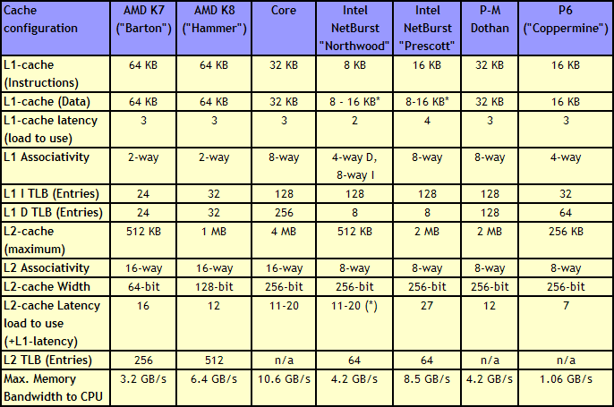
Core gave a 4 MB Level 2 cache between two cores, with a 12-14 cycle access time. This allows each core to use more than 2MB of L2 if needed, something Presler did not allow. Each core also has a 3-cycle 32KB instruction + 32KB data cache, compared to the super small Netburst, and also supports 256 entries in the L1 data TLB, compared to 8. Both the L1 and L2 are accessible by a 256-bit interface, giving good bandwidth to the core.
Note that AMD’s K8 still has a few advantages over Core. The 2-way 64KB L1 caches on AMD’s K8 have a slightly better hit rate to the 8-way 32KB L1 caches on Core, with a similar latency. AMD’s K8 also used an on-die memory controller, lowering memory latency significantly, despite the faster FSB of Intel Core (relative to Netburst) giving a lower latency to Core. As stated in our microarchitecture overview at the time, Athlon 64 X2s memory advantage had gotten smaller, but a key element to the story is that these advantages were negated by other memory sub-system metrics, such as prefetching. Measured by ScienceMark, the Core microarchitecture’s L1 cache delivers 2x bandwidth, and the L2 cache is about 2.5x faster, than the Athlon one.


158 Comments
View All Comments
Akrovah - Wednesday, July 27, 2016 - link
My old E6700 is still alive and kicking. I only just replaced it as my primary system when Devil's Canyon came along. Still use it for my four year old's "first computer."djayjp - Wednesday, July 27, 2016 - link
Not a particle physicist, nor electrical engineer, so just some pie in the sky wondering here, but wouldn't it be possible to build transistors using carbon nanotubes, or light itself (using nano sized mirrors/interferometers, like DLP) or even basing the transistor gates off of protons/sub atomic particles?michael2k - Wednesday, July 27, 2016 - link
I think a more interesting question is using glass as a substrate. Imagine printing nand, CPU, GPU, ram, and along the bezels of a smartphone.That reduces a phone to six components: a display, a transducer for sound, a mic, a battery, a radio, and a chassis, which would have all the antennas.
joex4444 - Wednesday, July 27, 2016 - link
Particle physicist here. Light has the tricky property that it travels at the speed of light so I can't imagine it working but perhaps I'm envisioning your concept differently than you are. For carbon nanotubes, you'll need a materials engineer or a condensed matter physicist.3DoubleD - Wednesday, July 27, 2016 - link
Materials/Semiconductor Physics Engineer here. The problem is not what we CAN do, the problem is what is economically possible at scale. For example, FinFETs were demonstrated at the turn of the century, but took all of those years to become (1) necessary - planar transistor were getting too leaky, and (2) possible to fabricate economically in large scales.Researchers have created smaller, faster transistors years ago, but it takes a lot of time and effort to develop the EUV or quadruple patterning technologies that enable these devices to be reliably and affordably manufactured.
So I think the problem in moving "beyond silicon" is not that we don't have alternatives, it is that we have many alternatives, we just don't know which will scale. It becomes less of a purely engineering problem and manufacturing business problem. When new technologies relied purely on the established silicon industry alone, you could reasonably extrapolate how much each new technology would cost as the nodes were scaled down. When we talk about using III-V FinFETs/ All Around Gates or graphene and carbon nanotubes, we don't really know how those things will scale with the existing processes as we move them from the laboratory to the manufacturing line.
I've been looking forward to this transition for years. People moan that it is the end of Moores Law, but that could be a good thing. Silicon is a great material for forming logic circuits for many reasons, but it also has many downsides. While silicon never reached 10 GHz (as Intel once predicted), other materials easily blow past 100 GHz transistor switching speeds. When the massive engines that work tirelessly to reduce our lithography nodes nm by nm are aimed at "the next big thing", we might be pleasantly surprised by a whole new paradigm of performance.
So what competes with modern day Si CMOS on speed, power usage, and cost? Nothing... yet!
djayjp - Thursday, July 28, 2016 - link
Yes, it's fascinating stuff. Thanks for reminding me about that. I recall now that I think it was graphene that enabled those insanely high switching speeds, due to its incredible conductivity/efficiency. Hopefully it can now be made economically feasible at some point! Imagine a the next GPU that is 10x smaller and operates at 100x the clock speed. A GTX 1080Ti x 1000! Finally we can do real time true global illumination ha....jeffry - Monday, August 1, 2016 - link
Thats a good point. Like, answering a question "are you willing to pay $800 for a new CPU to double the computers speed?" Most consumers say no. It all comes down to the mass market price.wumpus - Thursday, August 4, 2016 - link
From the birth of the Univac until 10 years ago, consumers consistently said YES! and plunked down their money. Doubling the (per thread) speed of a core2duo is going to cost more than $800. Also the cost of the RAM on servers is *WAY* more than $800, so you can expect if Intel could double the power of each core, they could crank prices up by at least $800 per core on Xeons. They can't, and neither can IBM or AMD.Jaybus - Thursday, July 28, 2016 - link
Sure, but that speed is dependent on the medium. There are some proposed optical transistors using electromagnetically induced transparency. Long way off. However, silicon photonics could change some things. Capacitance is the killer for electronic interconnects, whether chip-to-chip or on-chip bus. An optical interconnect could greatly increase bandwidth without increasing the chip's power dissipation. I think an electronic-photonic hybrid is more likely, since silicon photonics components can be made on a CMOS process. We are already beginning to see optical PCI Express being deployed. I could definitely see a 3D approach where 2D electronic layers are connected through an optical rather than electronic bus.djayjp - Thursday, July 28, 2016 - link
Yes, transparency, like polarized windows that either become transparent or opaque when a current is applied (to the liquid crystals?). I wonder how small they could be made. It would be incredibly power efficient I would think.