Ten Year Anniversary of Core 2 Duo and Conroe: Moore’s Law is Dead, Long Live Moore’s Law
by Ian Cutress on July 27, 2016 10:30 AM EST- Posted in
- CPUs
- Intel
- Core 2 Duo
- Conroe
- ITRS
- Nostalgia
- Time To Upgrade
Core: It’s all in the Prefetch
In a simple CPU design, instructions are decoded in the core and data is fetched from the caches. In a perfect world, such as the Mill architecture, the data and instructions are ready to go in the lowest level cache at all times. This allows for the lowest latency and removes a potential bottleneck. Real life is not that rosy, and it all comes down to how the core can predict what data it needs and has enough time to drag it down to the lowest level of cache it can before it is needed. Ideally it needs to predict the correct data, and not interfere with memory sensitive programs. This is Prefetch.
The Core microarchitecture added multiple prefetchers in the design, as well as improving the prefetch algorithms, to something not seen before on a consumer core. For each core there are two data and one instruction prefetchers, plus another couple for the L2 cache. That’s a total of eight for a dual core CPU, with instructions not to interfere with ‘on-demand’ bandwidth from running software.
One other element to the prefetch is tag lookup for cache indexing. Data prefetchers do this, as well as running software, so in order to avoid a higher latency for the running program, the data prefetch uses the store port to do this. As a general rule (at least at the time), loads happen twice as often as stores, meaning that the store port is generally more ‘free’ to be used for tag lookup by the prefetchers. Stores aren’t critical for most performance metrics, unless the system can’t process stores quickly enough that it backs up the pipeline, but in most cases the rest of the core will be doing things regardless. The cache/memory sub-system is in control for committing the store through the caches, so as long as this happens eventually the process works out.
Core: More Cache Please
Without having access to a low latency data and instruction store, having a fast core is almost worthless. The most expensive SRAMs sit closest to the execution ports, but are also the smallest due to physical design limitations. As a result, we get a nested cache system where the data you need should be in the lowest level possible, and accesses to higher levels of cache are slightly further away. Any time spent waiting for data to complete a CPU instruction is time lost without an appropriate way of dealing with this, so large fast caches are ideal. The Core design, over the previous Netburst family but also over AMD’s K8 ‘Hammer’ microarchitecture, tried to swat a fly with a Buick.
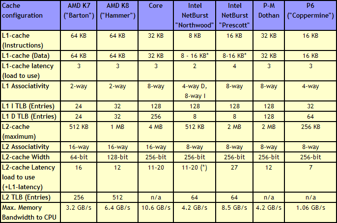
Core gave a 4 MB Level 2 cache between two cores, with a 12-14 cycle access time. This allows each core to use more than 2MB of L2 if needed, something Presler did not allow. Each core also has a 3-cycle 32KB instruction + 32KB data cache, compared to the super small Netburst, and also supports 256 entries in the L1 data TLB, compared to 8. Both the L1 and L2 are accessible by a 256-bit interface, giving good bandwidth to the core.
Note that AMD’s K8 still has a few advantages over Core. The 2-way 64KB L1 caches on AMD’s K8 have a slightly better hit rate to the 8-way 32KB L1 caches on Core, with a similar latency. AMD’s K8 also used an on-die memory controller, lowering memory latency significantly, despite the faster FSB of Intel Core (relative to Netburst) giving a lower latency to Core. As stated in our microarchitecture overview at the time, Athlon 64 X2s memory advantage had gotten smaller, but a key element to the story is that these advantages were negated by other memory sub-system metrics, such as prefetching. Measured by ScienceMark, the Core microarchitecture’s L1 cache delivers 2x bandwidth, and the L2 cache is about 2.5x faster, than the Athlon one.


158 Comments
View All Comments
Nameofuser44 - Wednesday, August 3, 2016 - link
Here I thought I was the only slow poke to not give up my C2D (4300) & ATI 5770 / 2GB ram /as a daily driver. Well here's to ten wonderful years!rarson - Thursday, August 4, 2016 - link
I'm still using a Core 2 Duo E8600 in my desktop. In an Abit P-35 Pro motherboard. The damn thing just works too well to get rid of, and I love the Abit board.rarson - Thursday, August 4, 2016 - link
Durr, it's the IP35 pro, P35 chipset.skidaddy - Friday, August 5, 2016 - link
My 10 year old E6600 with EVGA board & EVGA/NVIDIA 295 video card is also a great space heater. CUDA on card extended utility of set up. Only limitation is no CPU video decoding limits streaming to 1440. Waiting for the Intel Kaby Lake or better on die Intel GPU to be able to handle 4K @ 60fps over HDMI not USB3(+).BoberFett - Friday, August 5, 2016 - link
I'm still rocking my C2D E6500. It does the job.johnpombrio - Friday, August 5, 2016 - link
The Core 2 architecture was developed in Israel by a Intel team working on mobile processors. Intel suddenly realized that they had a terrific chip on their hands and ran with it. The rest is history.http://www.seattletimes.com/business/how-israel-sa...
FourEyedGeek - Monday, August 8, 2016 - link
How do you think one of those first Core processors would fare if fabricated at Intels 10nm process?Could they lower voltage or increase performance significantly?
Visual - Monday, August 8, 2016 - link
So a 10 year old chip is about half the performance of today's price equivalent. I'd have hoped today's tech to be more like 10 times better instead of just 2.