Ten Year Anniversary of Core 2 Duo and Conroe: Moore’s Law is Dead, Long Live Moore’s Law
by Ian Cutress on July 27, 2016 10:30 AM EST- Posted in
- CPUs
- Intel
- Core 2 Duo
- Conroe
- ITRS
- Nostalgia
- Time To Upgrade
Core: Out of Order and Execution
After Prefetch, Cache and Decode comes Order and Execution. Without rehashing discussions of in-order vs. out-of-order architectures, typically a design with more execution ports and a larger out-of-order reorder buffer/cache can sustain a higher level of instructions per clock as long as the out-of-order buffer is smart, data can continuously be fed, and all the execution ports can be used each cycle. Whether having a super-sized core is actually beneficial to day-to-day operations in 2016 is an interesting point to discuss, during 2006 and the Core era it certainly provided significant benefits.
As Johan did back in the original piece, let’s start with semi-equivalent microarchitecture diagrams for Core vs. K8:
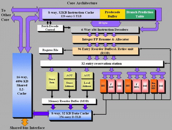
Intel Core
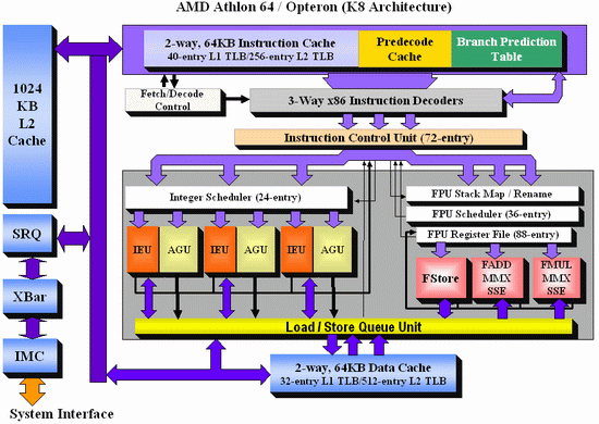
AMD K8
For anyone versed in x86 design, three differences immediately stand out when comparing the two. First is the reorder buffer, which for Intel ranks at 96 entries, compared to 72 for AMD. Second is the scheduler arrangement, where AMD uses split 24-entry INT and 36-entry FP schedulers from the ‘Instruction Control Unit’ whereas Intel has a 32-entry combined ‘reservation station’. Third is the number of SSE ports: Intel has three compared to two from AMD. Let’s go through these in order.
For the reorder buffers, with the right arrangement, bigger is usually better. Make it too big and it uses too much silicon and power however, so there is a fine line to balance between them. Also, the bigger the buffer it is, the less of an impact it has. The goal of the buffer is to push decoded instructions that are ready to work to the front of the queue, and make sure other instructions which are order dependent stay in their required order. By executing independent operations when they are ready, and allowing prefetch to gather data for instructions still waiting in the buffer, this allows latency and bandwidth issues to be hidden. (Large buffers are also key to simultaneous multithreading, which we’ll discuss in a bit as it is not here in Core 2 Duo.) However, when the buffer has the peak number of instructions being sent to the ports every cycle already, having a larger buffer has diminishing returns (the design has to keep adding ports instead, depending on power/silicon budget).
For the scheduler arrangements, using split or unified schedulers for FP and INT has both upsides and downsides. For split schedulers, the main benefit is entry count - in this case AMD can total 60 (24-INT + 36-FP) compared to Intel’s 32. However, a combined scheduler allows for better utilization, as ports are not shared between the split schedulers.
The SSE difference between the two architectures is exacerbated by what we’ve already discussed – macro-op fusion. The Intel Core microarchitecture has 3 SSE units compared to two, but also it allows certain SSE packed instructions to execute within one instruction, due to fusion, rather than two. Two of the Intel’s units are symmetric, with all three sporting 128-bit execution rather than 64-bit on K8. This means that K8 requires two 64-bit instructions whereas Intel can absorb a 128-bit instruction in one go. This means Core can outperform K8 on 128-bit SSE on many different levels, and for 64-bit FP SSE, Core can do 4 DP per cycle, whereas Athlon 64 can do 3.
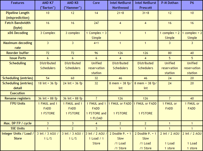
One other metric not on the diagram comes from branch prediction. Core can sustain one branch prediction per cycle, compared to one per two cycles on previous Intel microarchitectures. This was Intel matching AMD in this case, who already supported one per cycle.


158 Comments
View All Comments
Ian Cutress - Tuesday, August 2, 2016 - link
To clarify, there was a typo in Johan's original review of the microarchitecture, specifically stating:'However, Core is clearly a descendant of the Pentium Pro,'
I've updated the article to reflect this, and was under the assumption that my source was correct at the point of doing my research.
wumpus - Tuesday, August 2, 2016 - link
Except that the Pentium Pro was the first chip with the P6 architecture. Pentium 2 was pretty much pentium pro with MMX, a higher clock rate, and slower [off chip but on slot] L2 cache. Pentium 3 was the same with more clock, more MMX (possibly SSE), and on chip (full speed) L2 cache.While I'd have to assume they would pull all the files from the Pentium 3 plans, I'd still call it "pentinium pro based" because that was where nearly all the architecture came from (with minor upgrades and bug fixes to the core in 2 and 3).
I'm still curious as to exactly how they pulled it off. My main theory is that they duplicated the block diagram of the P6, and then verified each block was correct (and exactly duplicated the P6 at a higher speed), then used the P6 verification to prove that if the blocks were all correct, they had a correct chip.
zodiacfml - Thursday, July 28, 2016 - link
Same here. I thought it was the design of the Pentium M (from Israel team) they got the Core from. It was that time that AMD is beating Intel's P4's in performance, efficiency, and price. After a few months, articles were posted with people able to overclock a Pentium M with the characteristics of the AMD CPU and, of course, beating Pentium 4's at much lower clock speeds. From there, the Intel Core was born out of the Pentium M's which is essentially the same only with higher TDP and clock speeds. Then came, the Core Duo, then the Core 2 Duo.I just can't remember where I read it though.
marty1980 - Wednesday, July 27, 2016 - link
I started college in electrical engineering; moved to software after an ee class using c++. I was very excited and confident in a DIY PC. I knew the Core 2 was on its way. I gathered parts from whatever computers I could scratch together; power supply, case, DVD drive, network card(s), HDDs ... Everything but Mobo, CPU, GPU and RAM - the brains.I bought an E6400 2.13GHz with a gigabyte mobo, 4GB 800MHz DDR2 and a Radeon x1650 Pro.
I just retired the CPU and Mobo in 2012/13 when I experimented with my current PC; an AMD APU + Ded GPU (dual graphics).
I'm excited to be looking at a future replacement for my PC. We're on the horizon of some interesting changes that I don't even understand (what was his article about? Lol).
just4U - Thursday, July 28, 2016 - link
I seem to recall from a casual glance at an article (on this site) back some 9 years ago.. That intel basically got lucky, or fluked as it were.. Something to do with what they were doing with the PentiumM which caused them to move away from the P3-4 stuff.. hum.. damned if I can remember though what it was about.FourEyedGeek - Tuesday, August 9, 2016 - link
Pentium 3 architecture was having difficulties increasing performance so they replaced it with Pentium 4s Netburst. They had their Israel department continue work on Pentium 3 that turned into the Pentium M.Hazly79 - Thursday, July 28, 2016 - link
surprised that my 2005-Pentium D 3ghz still can run Diablo 3 (2012) at minimum setting pair with Nvidia GT 710 ($35 card )Really great optimization from Blizzard ent. team...
AnnonymousCoward - Thursday, July 28, 2016 - link
Yeah, but too bad the game sucks. Jay doubled it.name99 - Thursday, July 28, 2016 - link
Two points:Firstly macro-op fusion is hardly an x86 exclusive these days. Many (all?) ARMv8 CPUs use it, as do the most recent POWER CPUs. Like the x86 case, it's used to fuse together pairs of instructions that commonly co-occur. Compare and branch is a common example, but other common examples in RISC are instruction pairs that are used to create large constants in a register, or to generate large constant offsets for loads/stores.
Secondly you suggest that the ROB is an expensive data structure. This is misleading. The ROB itself is primarily a FIFO and can easily be grown. The problem is that storing more items in the ROB requires more physical registers and more load/store queue entries, and it is THESE structures that are difficult and expensive to grow. This suggests that using alternative structures for the load/store queues, and alternative mechanisms for scavenging physical registers could allow for much larger ROBs, and in fact Intel has published a lot of work on this (but has so far done apparently nothing with this research, even though the first such publications were late 90s --- I would not be surprised if Apple provides us with a CPU implementing these ideas before Intel does).
Ian Cutress - Tuesday, August 2, 2016 - link
It wasn't written about to the exclusion of all other microarchitectures, it was written about focusing on x86 back in 2006. At the time, the ROB was described as expensive by Intel, through I appreciate that might have changed.