Ten Year Anniversary of Core 2 Duo and Conroe: Moore’s Law is Dead, Long Live Moore’s Law
by Ian Cutress on July 27, 2016 10:30 AM EST- Posted in
- CPUs
- Intel
- Core 2 Duo
- Conroe
- ITRS
- Nostalgia
- Time To Upgrade
Core: Out of Order and Execution
After Prefetch, Cache and Decode comes Order and Execution. Without rehashing discussions of in-order vs. out-of-order architectures, typically a design with more execution ports and a larger out-of-order reorder buffer/cache can sustain a higher level of instructions per clock as long as the out-of-order buffer is smart, data can continuously be fed, and all the execution ports can be used each cycle. Whether having a super-sized core is actually beneficial to day-to-day operations in 2016 is an interesting point to discuss, during 2006 and the Core era it certainly provided significant benefits.
As Johan did back in the original piece, let’s start with semi-equivalent microarchitecture diagrams for Core vs. K8:
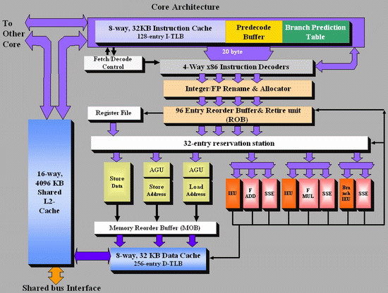
Intel Core
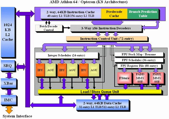
AMD K8
For anyone versed in x86 design, three differences immediately stand out when comparing the two. First is the reorder buffer, which for Intel ranks at 96 entries, compared to 72 for AMD. Second is the scheduler arrangement, where AMD uses split 24-entry INT and 36-entry FP schedulers from the ‘Instruction Control Unit’ whereas Intel has a 32-entry combined ‘reservation station’. Third is the number of SSE ports: Intel has three compared to two from AMD. Let’s go through these in order.
For the reorder buffers, with the right arrangement, bigger is usually better. Make it too big and it uses too much silicon and power however, so there is a fine line to balance between them. Also, the bigger the buffer it is, the less of an impact it has. The goal of the buffer is to push decoded instructions that are ready to work to the front of the queue, and make sure other instructions which are order dependent stay in their required order. By executing independent operations when they are ready, and allowing prefetch to gather data for instructions still waiting in the buffer, this allows latency and bandwidth issues to be hidden. (Large buffers are also key to simultaneous multithreading, which we’ll discuss in a bit as it is not here in Core 2 Duo.) However, when the buffer has the peak number of instructions being sent to the ports every cycle already, having a larger buffer has diminishing returns (the design has to keep adding ports instead, depending on power/silicon budget).
For the scheduler arrangements, using split or unified schedulers for FP and INT has both upsides and downsides. For split schedulers, the main benefit is entry count - in this case AMD can total 60 (24-INT + 36-FP) compared to Intel’s 32. However, a combined scheduler allows for better utilization, as ports are not shared between the split schedulers.
The SSE difference between the two architectures is exacerbated by what we’ve already discussed – macro-op fusion. The Intel Core microarchitecture has 3 SSE units compared to two, but also it allows certain SSE packed instructions to execute within one instruction, due to fusion, rather than two. Two of the Intel’s units are symmetric, with all three sporting 128-bit execution rather than 64-bit on K8. This means that K8 requires two 64-bit instructions whereas Intel can absorb a 128-bit instruction in one go. This means Core can outperform K8 on 128-bit SSE on many different levels, and for 64-bit FP SSE, Core can do 4 DP per cycle, whereas Athlon 64 can do 3.
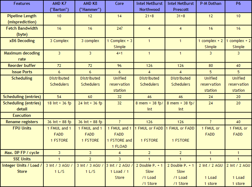
One other metric not on the diagram comes from branch prediction. Core can sustain one branch prediction per cycle, compared to one per two cycles on previous Intel microarchitectures. This was Intel matching AMD in this case, who already supported one per cycle.


158 Comments
View All Comments
Hazly79 - Wednesday, July 27, 2016 - link
History of Intel processori 386 1986
i 486 1989 - 94
Pentium / MMX 1994 - 96
Pentium II 1997
Pentium III 1999
Pentium 4 / 4 HT 2002 - 04
Pentium D 2005
Core [ 2 ] Duo 2006 - 08
Core [ 2 ] Quad 2007 - 08
Core [ i ] Nehalem 2008
Core [ i ] Westmere 2009
Core [ i ] Sandy Bridge 2011
Core [ i ] Ivy Bridge 2012
Core [ i ] Haswell 2013
Core [ i ] Broadwell 2014
Core [ i ] Skylake 2015
Core [ i ] Kabylake 2016
AnnonymousCoward - Wednesday, July 27, 2016 - link
So how many decades will it take til cpus have significantly faster single-thread than a 6700K@4.4GHz?Notmyusualid - Thursday, July 28, 2016 - link
+1Mr Perfect - Wednesday, July 27, 2016 - link
Hmm. We've got an ancient 2007 Macbook with a 2GHz C2D(T7200 I think) in it that's still used for web browsing on a daily basis. Upgrading it to 4GB of ram and a SSD made it surprisingly capable.It's not all a bed of roses though, as random things will come out of left field and floor it. I think it's mostly flash heavy sites, but Twitter and Vine freak it out a little.
Hulk - Wednesday, July 27, 2016 - link
I vividly remember the anticipation and hype leading up to the C2D release. The the years of struggle Intel had with Netburst before Conroe. It was what I consider the end of the golden age of the CPU. Great job Ian!Impulseman45 - Wednesday, July 27, 2016 - link
Ah, it wasn't the Pentium Pro it was based on. The Core family was a direct descendant of the Pentium 3 Tualatin. They stopped sales of the of the Pentium 3 Tualatin because it was outperforming the Pentium 4. They migrated that technology to the notebook line as it was much more efficient. It became the Pentium M. When Intel realized that the Pentium 4 Netburst architecture was a dead end and they needed a new chip to go up against AMD, they sourced their notebook chips to build the Core series. See this is what is called re-writing history. Come on guys, it is very well known that they sourced the Pentium M Yohan for the Core series. I do not know who did your research but it is all wrong. Go back and recheck your information. The Pentium Pro was the granddaddy of all the Pentium 2 and 3 chips so yeah, you can point to that chip in a vague way as the ancestor. But the Pentium 4 can as well well. So to be to the point, the core lines DNA goes back directly to the Pentium 3 Tualatin, So we have all been using very, very hopped up Pentium 3s the last 10 years. The Tualatin was an excellent chip. It overclock like crazy. There were Celeron and Sever P3 versions and all of them beat the hell out of the P4. Its know reason Intel had to kill it. Do more research so you can post accurate articles, please.Michael Bay - Thursday, July 28, 2016 - link
>teaching AT about CPU architecturesDamn it, you`re a riot!
Impulseman45 - Thursday, July 28, 2016 - link
These are not the original AT guys, they are all new people and they are not doing the research they should be doing. This is how history can get changed. People look to a reputable tech site that got something wrong and its written in stone. Well AT says this is how it is, even if they are wrong. Go check the history directly from Intel, This article is wrong and that is a fact, period. I felt it just needed to be called out on.natenu - Monday, August 1, 2016 - link
Refreshing to see this comment. HT was a marketing joke to keep up with clock rate shoppers.wumpus - Tuesday, August 2, 2016 - link
When Dave Barry jokes about "speed is measured in Megahertz" you know you are ripe for some marketing in your engineering.