NVIDIA Announces the GeForce GTX 1000 Series: GTX 1080 and GTX 1070 Arrive In May & June
by Ryan Smith on May 7, 2016 3:25 AM EST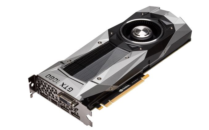
After many months of speculation – and more than a little anticipation – at an event in Austin, Texas this evening, NVIDIA announced the next generation of GeForce video cards, the GeForce 1000 series. Powered by the company’s new Pascal architecture and built on TSMC’s 16nm FinFET process, NVIDIA is promising that the 1000 series will set a new high bar for performance and efficiency while also offering a collection of new features to further set it apart from its predecessors.
The first two cards out of the gate will be NVIDIA’s high-end cards, the GTX 1080 and GTX 1070. 1080p jokes aside, these are straightforward successors to what has now been NVIDIA’s product stack naming scheme since 2010, with the GTX 1080 representing their new high-end card while the GTX 1070 is a cheaper card meant to hit the enthusiast sweet spot. These cards will be launching over the next month, with GTX 1080 hitting the market May 27th, and GTX 1070 two weeks later, on June 10th. They will be priced at $599 and $379 respectively.
| NVIDIA GPU Specification Comparison | ||||||
| GTX 1080 | GTX 1070 | GTX 980 | GTX 780 | |||
| CUDA Cores | 2560 | (Fewer) | 2048 | 2304 | ||
| Texture Units | 160? | (How many?) | 128 | 192 | ||
| ROPs | 64 | (Good question) | 64 | 48 | ||
| Core Clock | 1607MHz | (Slower) | 1126MHz | 863MHz | ||
| Boost Clock | 1733MHz | (Again) | 1216MHz | 900Mhz | ||
| TFLOPs (FMA) | 9 TFLOPs | 6.5 TFLOPs | 5 TFLOPs | 4.1 TFLOPs | ||
| Memory Clock | 10Gbps GDDR5X | GDDR5 | 7Gbps GDDR5 | 6Gbps GDDR5 | ||
| Memory Bus Width | 256-bit | ? | 256-bit | 256-bit | ||
| VRAM | 8GB | 8GB | 4GB | 3GB | ||
| FP64 | ? | ? | 1/32 FP32 | 1/24 FP32 | ||
| TDP | 180W | ? | 165W | 250W | ||
| GPU | "GP104" | "GP104" | GM204 | GK110 | ||
| Transistor Count | 7.2B | 7.2B | 5.2B | 7.1B | ||
| Manufacturing Process | TSMC 16nm | TSMC 16nm | TSMC 28nm | TSMC 28nm | ||
| Launch Date | 05/27/2016 | 06/10/2016 | 09/18/2014 | 05/23/2013 | ||
| Launch Price | MSRP: $599 Founders $699 |
MSRP:$379 Founders: $449 |
$549 | $649 | ||
The Pascal Architecture & "GP104"
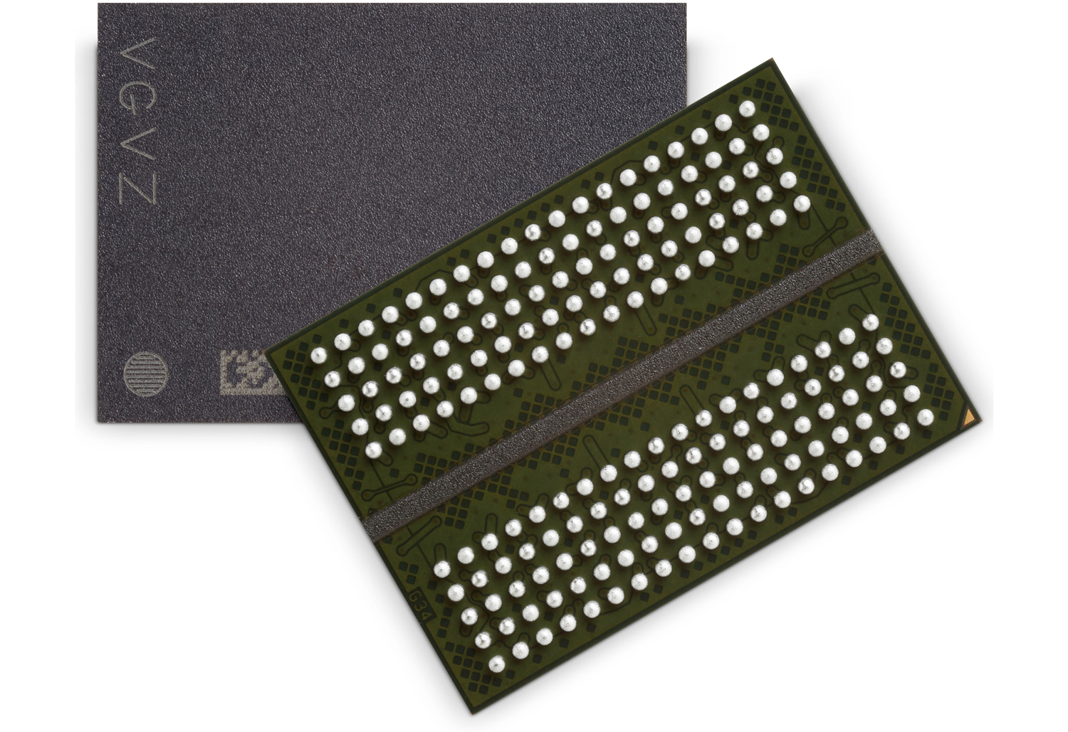
While NVIDIA’s public presentation this evening was not a deep dive technical presentation – and as such there are still a number of blanks to fill in later – we still have a bunch of information to dive into. First and foremost, let’s talk about the GPU. NVIDIA is not using the GPU’s name, but in their presentation they did confirm that it had 7.2B transistors, and as such making it clear that this is a new Pascal GPU and not a cut-down version of the 15.3B transistor GP100. For the moment I am assuming this is GP104 – following NVIDIA’s traditional naming scheme – but this is subject to confirmation.
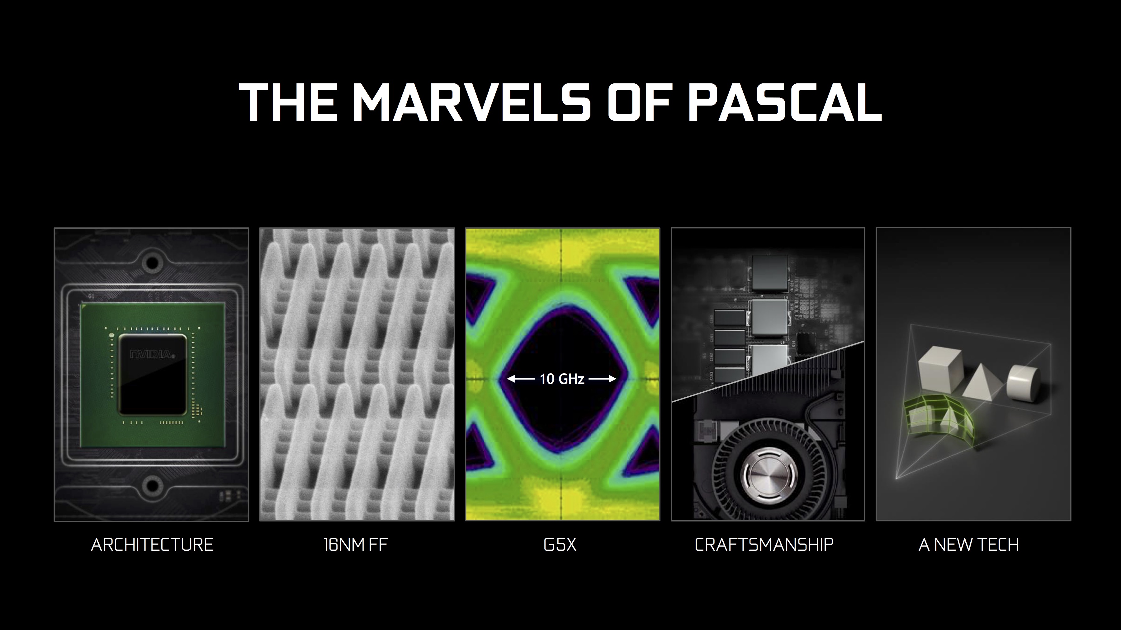
GP104, as you’d expect, is being produced by long-time partner TSMC on their 16nm FinFET process, making this the first consumer GPU built on the 14/16nm processes to ship when it hits the streets later this month. It goes without saying that the GPU industry has been stuck on 28nm for much longer than usual – GK104 to GP104 will be 4 years and 2 months – so this a long-awaited opportunity to jump to a smaller feature process and reap the power and performance benefits that entails.
At this time we don’t know GP104’s die size, but at fewer than half the transistors than GP100 it’s a safe bet that this is a die size in-line with previous first-run 104 GPUs such as GK104 and GF104, which were 294mm2 and 332mm2 respectively. GM204, by comparison, was a larger GPU, coming later in the lifetime of the 28nm process. What this means is that NVIDIA has spent some of their 16nm savings on bringing the die size back down as compared to GM204. 16nm is still relatively early in its life, and unlike Tesla P100 where customers will pay very high prices for early access to a lower-yielding chip, for consumer parts NVIDIA has needed to be more conservative. On that note, at this time it is not clear whether the GP104 in GTX 1080 is a fully enabled GP104 GPU, though traditionally it has been.
Pascal of course isn’t just NVIDIA’s 16nm architecture, but it is their successor to Maxwell. We know from NVIDIA’s previous Tesla P100 announcement that the company has opted to pay special attention to CUDA Core efficiency with Pascal, improving the throughput of the architecture as opposed to adding a significant number of additional CUDA cores. As a result, like previous architectural shifts, core-for-core comparisons are going to be tricky thanks to GP104 hitting a higher percentage of its theoretical throughput in practice. I’m still waiting on more technical details on GP104, and whether certain improvements like the larger register file have been carried over. Otherwise NVIDIA is promoting a 2x efficiency increase in Pascal versus Maxwell for gaming purposes.
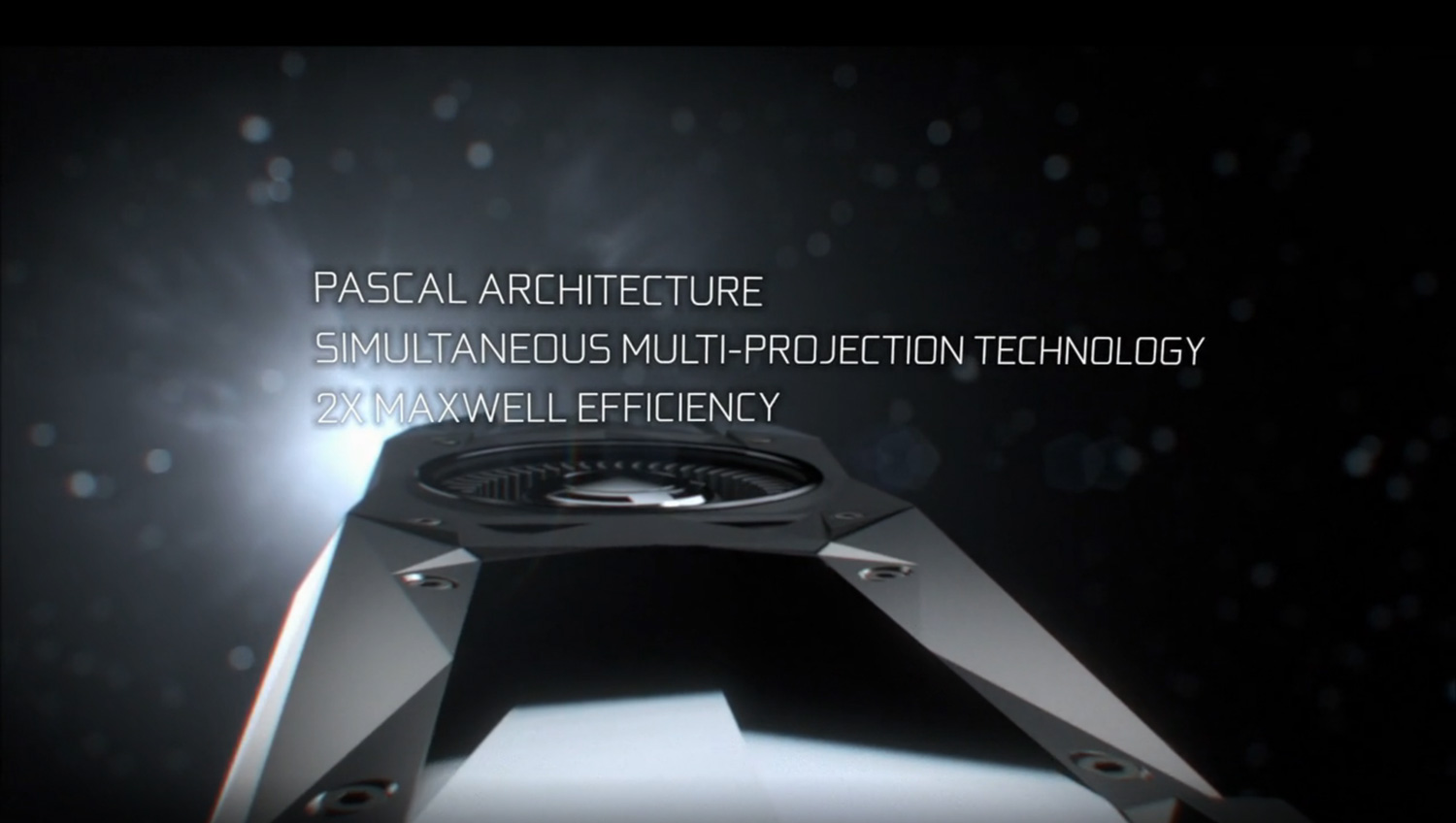
On top of that 2x efficiency improvement – and how NVIDIA gets to their claimed 3x efficiency improvement over GTX Titan X – Pascal implement some new features that developers can tap for improved performance. Key among these is Simultaneous Multi-Projection, a technology that allows Pascal to create up to 16 viewports. NVIDIA is promoting the tech as being especially well suited for more efficient implementations of VR lens distortion correction (Lends Matched Shading) and rendering the same scene twice in VR – once for each eye – in a single pass (Single Pass Stereo), along with easier correction for distortion when using a multi-monitor setup.
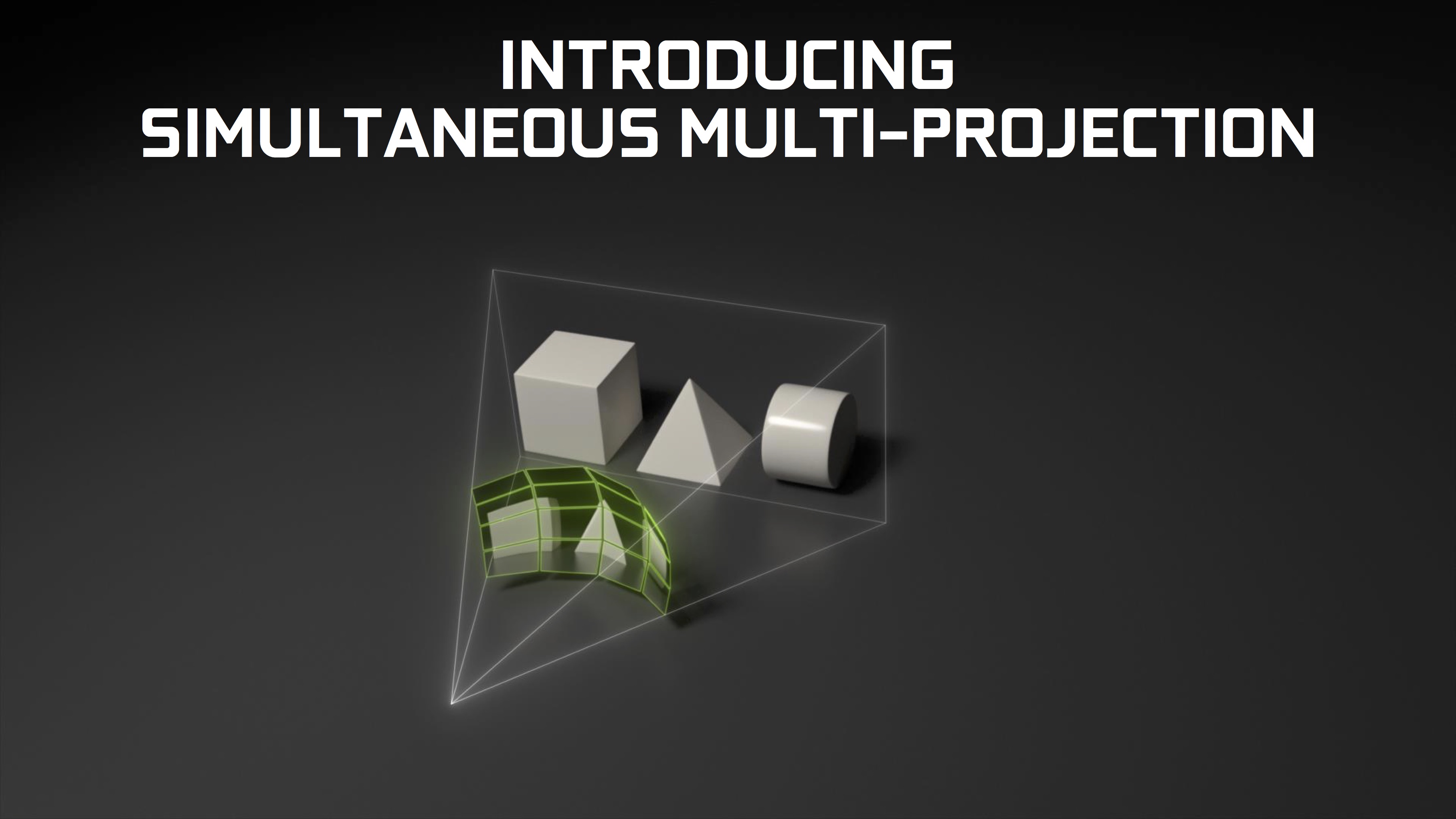
Truth be told at this time I do not know how Simultaneous Multi-Projection Differs from NVIDIA’s previously announced features for Maxwell: Multi-Projection Acceleration and Multi-Res Shading. NVIDIAs description of SMP is very similar to these, as are the underlying algorithmic tweaks of reprojecting geometry and shading different parts of a frame at different resolutions.
A final new GPU-level feature on GP104 and the new GTX 1000 series cards is GPU Boost 3.0. Information about this is limited, but NVIDIA is saying that it supports more advanced overclocking functionality than has been present over the last couple of years with GPU Boost 2.0.
Meanwhile from a feature standpoint, NVIDIA has confirmed that GP104 cards will be DirectX feature level FL12_1 capable. Though as FL12_1 allows multiple tiers of certain sub-features, it’s not clear at this time whether Pascal supports higher tiers of those features. On the display side of matters, GP104’s display controller will support the newer DisplayPort 1.3 and 1.4 standards. Officially the cards are being called “DisplayPort 1.2 Certified, DisplayPort 1.3/1.4 Ready,” the distinction being that the latter is not currently certified, though I suspect the DP 1.3/1.4 certification process may itself not be ready yet.
Turning over from the GPU to memory, whereas GP100 was the first NVIDIA GPU to support HBM2, GP104 will be the first GPU to support GDDR5X. An updated version of the GDDR5 standard originally announced by Micron and more recently approved by the JEDEC, GDDR5X iterates on the technology to improve memory bandwidth. At a basic level, GDDR5X increases the overall capacity of the memory bus by moving from double-pumping (DDR) to quad-pumping (QDR), pairing this change with a larger memory prefetch to feed the faster memory bus, all while avoiding a more painful/difficult increase in the memory core clock.
GDDR5X will allow NVIDIA (and other vendors) to increase memory bandwidth while following more traditional GDDR5-style memory designs, rather than more complex designs like HBM. At the same time this also allows a single GPU to easily support a newer memory standard and the older GDDR5 standard at the same time, as the latter will remain a cheaper memory technology for some time. NVIDIA will be putting this feature to good use in enabling the GTX 1080 to run GDDR5X, while the GTX 1070 will run GDDR5.
Finally, not touched upon in NVIDIA’s initial presentation is that GP104 will use a newer version of NVIDIA’s SLI technology. Dubbed SLI HB (High Bandwidth), SLI HB will double the amount of bandwidth available between paired cards. At the same time this change will require a new SLI HB bridge, presumably to be compliant with the tighter signal integrity requirements a higher bandwidth link would require. NVIDIA is producing the new rigid bridge with their usual flair for industrial design, and so far I have not heard anything about the older non-rigid bridge making a return. In which case buyers will need bridges specifically sized for the slot arrangement of their board.


234 Comments
View All Comments
nevcairiel - Sunday, May 8, 2016 - link
Then wait until someone can confirm this. Like I said they never listed those things in the specs of any previous GPU, so it not being in there now means nothing.mdriftmeyer - Sunday, May 8, 2016 - link
They claim 10 bit for DirectX, and even XOrg on Linux, but it's a bust.https://devtalk.nvidia.com/default/topic/771081/li...
Murloc - Sunday, May 8, 2016 - link
we don't know if it's included but it likely is.That's hardly grounds for curb stomping.
The rest (mostly perf/watt) is all yet to be seen.
D. Lister - Sunday, May 8, 2016 - link
For 10-bit color support, you need a Quadro or Firepro. No point in putting such functionality in a consumer product where screen response time is often far more important than color accuracy.bill44 - Sunday, May 8, 2016 - link
10 bit is not just for color accuracy, it's essential for HDR. HDR is very important for games and UHD BD playback (which is coming to PCs). Polaris promised 10 bit HDR, HDR monitor will also be available by the end of the year.Also, there are many who will buy GTX 1080 for madVR etc., not just for games. So yes, going forward, 10 bit is essential in a consumer card. There are more monitors available now with QD technology, which will help with WCG and P3 gamut and beyond is now part of iMac's, and future HFR display technology (like Dell OLED 120Hz monitor).
As we're going forward, DP1.3/1.4 over USB Type-C will become available too. Unfortunately, TB3 can only support DP1.2 in it's present form.
nevcairiel - Sunday, May 8, 2016 - link
Since you already named madVR, 10-bit already works using any current NVIDIA card, so thats not going to change.bill44 - Sunday, May 8, 2016 - link
I mean proper systemwide driver that works with windowed programs and major apps lfrom Adobe. I know the limitations as far as Windows go (MS need to sort out Color Manegement once & for all, preferably using systemwide 3D LUTs), Mac's are better in this regard, however, everything starts with proper hardware and driver support.nevcairiel - Sunday, May 8, 2016 - link
Honestly the only people that needs this in Adobe apps are content producers, and they might as well buy a Quadro/FirePro.Its otherwise just a Microsoft limitation, they could easily drive the compositor in 10-bits and allow apps to use that.
bill44 - Sunday, May 8, 2016 - link
Thanks. What's the difference between HDMI 2.0a and (here) 2.0b? Some sites say level 'b' is only 10.8Gb/s, others disagree. Does it matter? Or should we just wait for 2.1 with dynamic metadata support?nevcairiel - Monday, May 9, 2016 - link
There is a bunch of confusion going around about that, since the naming is slightly confusing.HDMI 2.0 had two levels, Level A and Level B. Level B is what all older NVIDIA GPUs offered, HDMI 1.4 speed and some HDMI 2.0 features, ie. 4k@60 using 4:2:0 chroma to get the bandwidth down.
HDMI 2.0a and HDMI 2.0b are not related to those two levels, but are improvements on the HDMI 2.0 standard. 2.0a adds (static) HDR support, but I'm not certain what 2.0b does, it doesn't seem documented much yet, perhaps not officially released yet.
Unfortunately some people used the 2.0a/2.0b naming for the two tier levels in the past, causing such confusion.
Admittedly it is possible that NVIDIA would also use the confusing naming, but considering they also claim DP 1.3 support at the same time, and previous NVIDIA GPUs had 18gbps HDMI chips already, it would seem rather odd to take a step back.