NVIDIA Announces the GeForce GTX 1000 Series: GTX 1080 and GTX 1070 Arrive In May & June
by Ryan Smith on May 7, 2016 3:25 AM EST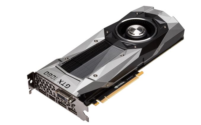
After many months of speculation – and more than a little anticipation – at an event in Austin, Texas this evening, NVIDIA announced the next generation of GeForce video cards, the GeForce 1000 series. Powered by the company’s new Pascal architecture and built on TSMC’s 16nm FinFET process, NVIDIA is promising that the 1000 series will set a new high bar for performance and efficiency while also offering a collection of new features to further set it apart from its predecessors.
The first two cards out of the gate will be NVIDIA’s high-end cards, the GTX 1080 and GTX 1070. 1080p jokes aside, these are straightforward successors to what has now been NVIDIA’s product stack naming scheme since 2010, with the GTX 1080 representing their new high-end card while the GTX 1070 is a cheaper card meant to hit the enthusiast sweet spot. These cards will be launching over the next month, with GTX 1080 hitting the market May 27th, and GTX 1070 two weeks later, on June 10th. They will be priced at $599 and $379 respectively.
| NVIDIA GPU Specification Comparison | ||||||
| GTX 1080 | GTX 1070 | GTX 980 | GTX 780 | |||
| CUDA Cores | 2560 | (Fewer) | 2048 | 2304 | ||
| Texture Units | 160? | (How many?) | 128 | 192 | ||
| ROPs | 64 | (Good question) | 64 | 48 | ||
| Core Clock | 1607MHz | (Slower) | 1126MHz | 863MHz | ||
| Boost Clock | 1733MHz | (Again) | 1216MHz | 900Mhz | ||
| TFLOPs (FMA) | 9 TFLOPs | 6.5 TFLOPs | 5 TFLOPs | 4.1 TFLOPs | ||
| Memory Clock | 10Gbps GDDR5X | GDDR5 | 7Gbps GDDR5 | 6Gbps GDDR5 | ||
| Memory Bus Width | 256-bit | ? | 256-bit | 256-bit | ||
| VRAM | 8GB | 8GB | 4GB | 3GB | ||
| FP64 | ? | ? | 1/32 FP32 | 1/24 FP32 | ||
| TDP | 180W | ? | 165W | 250W | ||
| GPU | "GP104" | "GP104" | GM204 | GK110 | ||
| Transistor Count | 7.2B | 7.2B | 5.2B | 7.1B | ||
| Manufacturing Process | TSMC 16nm | TSMC 16nm | TSMC 28nm | TSMC 28nm | ||
| Launch Date | 05/27/2016 | 06/10/2016 | 09/18/2014 | 05/23/2013 | ||
| Launch Price | MSRP: $599 Founders $699 |
MSRP:$379 Founders: $449 |
$549 | $649 | ||
The Pascal Architecture & "GP104"
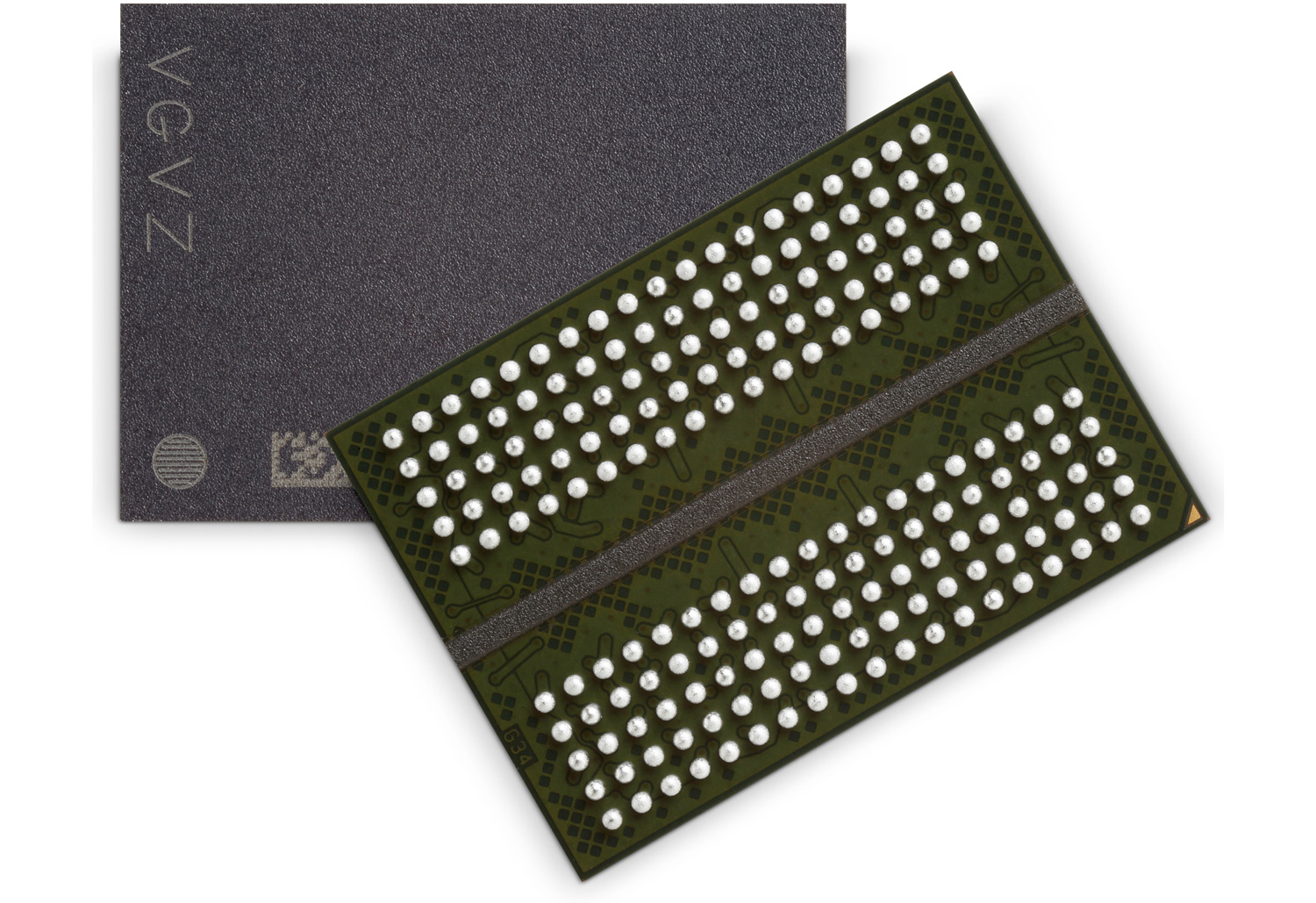
While NVIDIA’s public presentation this evening was not a deep dive technical presentation – and as such there are still a number of blanks to fill in later – we still have a bunch of information to dive into. First and foremost, let’s talk about the GPU. NVIDIA is not using the GPU’s name, but in their presentation they did confirm that it had 7.2B transistors, and as such making it clear that this is a new Pascal GPU and not a cut-down version of the 15.3B transistor GP100. For the moment I am assuming this is GP104 – following NVIDIA’s traditional naming scheme – but this is subject to confirmation.
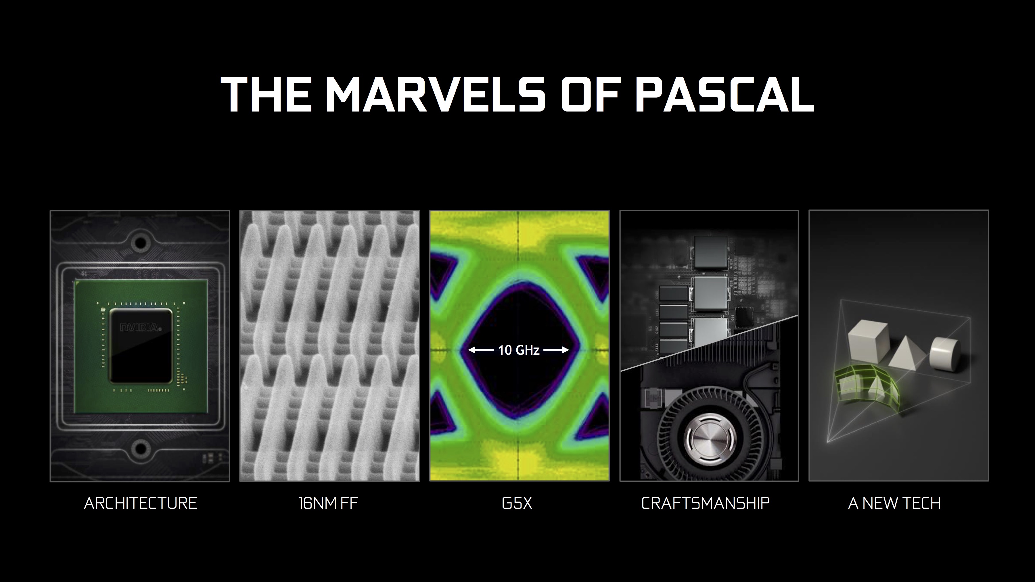
GP104, as you’d expect, is being produced by long-time partner TSMC on their 16nm FinFET process, making this the first consumer GPU built on the 14/16nm processes to ship when it hits the streets later this month. It goes without saying that the GPU industry has been stuck on 28nm for much longer than usual – GK104 to GP104 will be 4 years and 2 months – so this a long-awaited opportunity to jump to a smaller feature process and reap the power and performance benefits that entails.
At this time we don’t know GP104’s die size, but at fewer than half the transistors than GP100 it’s a safe bet that this is a die size in-line with previous first-run 104 GPUs such as GK104 and GF104, which were 294mm2 and 332mm2 respectively. GM204, by comparison, was a larger GPU, coming later in the lifetime of the 28nm process. What this means is that NVIDIA has spent some of their 16nm savings on bringing the die size back down as compared to GM204. 16nm is still relatively early in its life, and unlike Tesla P100 where customers will pay very high prices for early access to a lower-yielding chip, for consumer parts NVIDIA has needed to be more conservative. On that note, at this time it is not clear whether the GP104 in GTX 1080 is a fully enabled GP104 GPU, though traditionally it has been.
Pascal of course isn’t just NVIDIA’s 16nm architecture, but it is their successor to Maxwell. We know from NVIDIA’s previous Tesla P100 announcement that the company has opted to pay special attention to CUDA Core efficiency with Pascal, improving the throughput of the architecture as opposed to adding a significant number of additional CUDA cores. As a result, like previous architectural shifts, core-for-core comparisons are going to be tricky thanks to GP104 hitting a higher percentage of its theoretical throughput in practice. I’m still waiting on more technical details on GP104, and whether certain improvements like the larger register file have been carried over. Otherwise NVIDIA is promoting a 2x efficiency increase in Pascal versus Maxwell for gaming purposes.
On top of that 2x efficiency improvement – and how NVIDIA gets to their claimed 3x efficiency improvement over GTX Titan X – Pascal implement some new features that developers can tap for improved performance. Key among these is Simultaneous Multi-Projection, a technology that allows Pascal to create up to 16 viewports. NVIDIA is promoting the tech as being especially well suited for more efficient implementations of VR lens distortion correction (Lends Matched Shading) and rendering the same scene twice in VR – once for each eye – in a single pass (Single Pass Stereo), along with easier correction for distortion when using a multi-monitor setup.
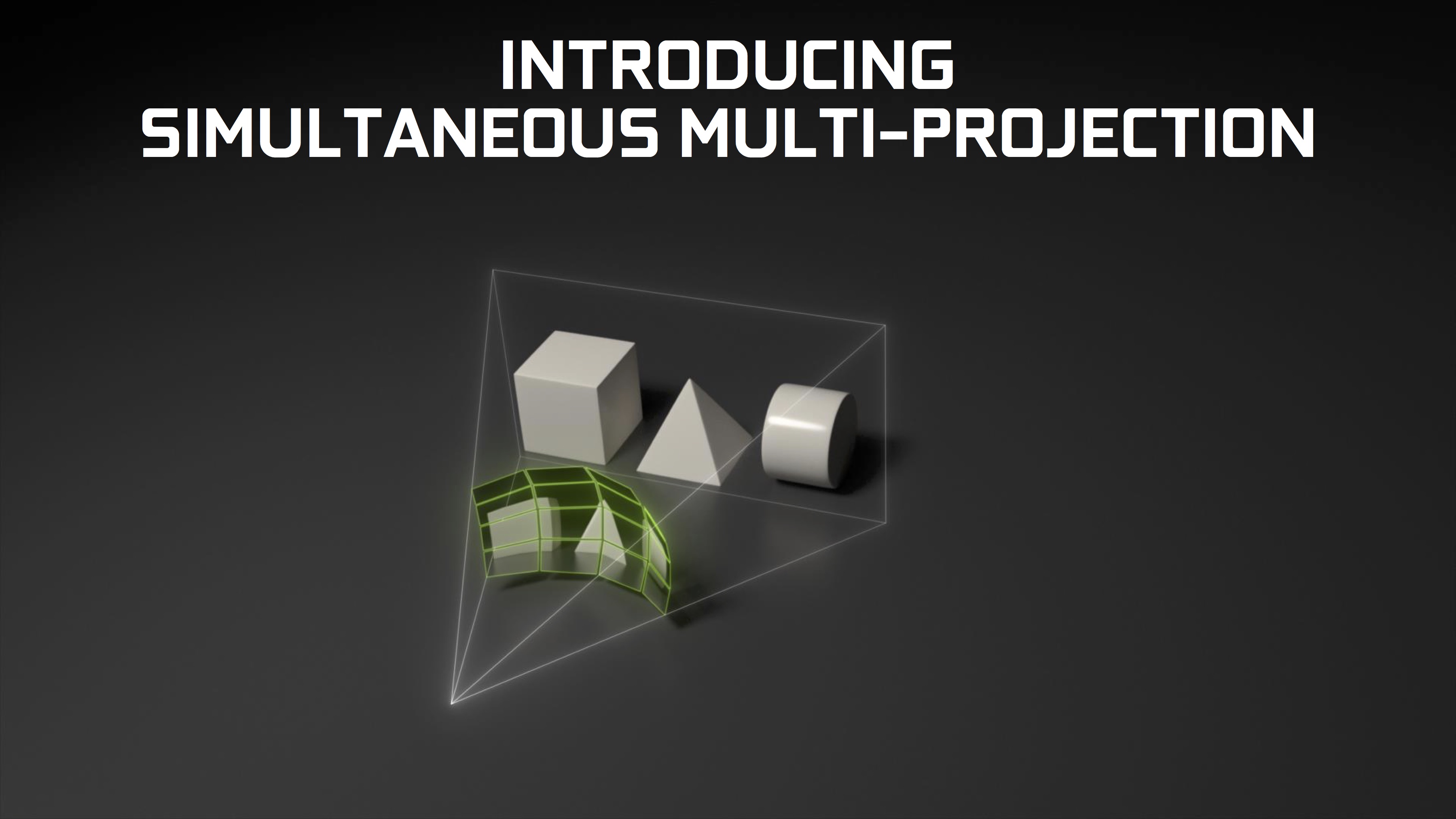
Truth be told at this time I do not know how Simultaneous Multi-Projection Differs from NVIDIA’s previously announced features for Maxwell: Multi-Projection Acceleration and Multi-Res Shading. NVIDIAs description of SMP is very similar to these, as are the underlying algorithmic tweaks of reprojecting geometry and shading different parts of a frame at different resolutions.
A final new GPU-level feature on GP104 and the new GTX 1000 series cards is GPU Boost 3.0. Information about this is limited, but NVIDIA is saying that it supports more advanced overclocking functionality than has been present over the last couple of years with GPU Boost 2.0.
Meanwhile from a feature standpoint, NVIDIA has confirmed that GP104 cards will be DirectX feature level FL12_1 capable. Though as FL12_1 allows multiple tiers of certain sub-features, it’s not clear at this time whether Pascal supports higher tiers of those features. On the display side of matters, GP104’s display controller will support the newer DisplayPort 1.3 and 1.4 standards. Officially the cards are being called “DisplayPort 1.2 Certified, DisplayPort 1.3/1.4 Ready,” the distinction being that the latter is not currently certified, though I suspect the DP 1.3/1.4 certification process may itself not be ready yet.
Turning over from the GPU to memory, whereas GP100 was the first NVIDIA GPU to support HBM2, GP104 will be the first GPU to support GDDR5X. An updated version of the GDDR5 standard originally announced by Micron and more recently approved by the JEDEC, GDDR5X iterates on the technology to improve memory bandwidth. At a basic level, GDDR5X increases the overall capacity of the memory bus by moving from double-pumping (DDR) to quad-pumping (QDR), pairing this change with a larger memory prefetch to feed the faster memory bus, all while avoiding a more painful/difficult increase in the memory core clock.
GDDR5X will allow NVIDIA (and other vendors) to increase memory bandwidth while following more traditional GDDR5-style memory designs, rather than more complex designs like HBM. At the same time this also allows a single GPU to easily support a newer memory standard and the older GDDR5 standard at the same time, as the latter will remain a cheaper memory technology for some time. NVIDIA will be putting this feature to good use in enabling the GTX 1080 to run GDDR5X, while the GTX 1070 will run GDDR5.
Finally, not touched upon in NVIDIA’s initial presentation is that GP104 will use a newer version of NVIDIA’s SLI technology. Dubbed SLI HB (High Bandwidth), SLI HB will double the amount of bandwidth available between paired cards. At the same time this change will require a new SLI HB bridge, presumably to be compliant with the tighter signal integrity requirements a higher bandwidth link would require. NVIDIA is producing the new rigid bridge with their usual flair for industrial design, and so far I have not heard anything about the older non-rigid bridge making a return. In which case buyers will need bridges specifically sized for the slot arrangement of their board.


234 Comments
View All Comments
kedesh83 - Saturday, May 7, 2016 - link
Edit: I meant that the 780 had 384bit memory bus, the graph above says 256.anubis44 - Saturday, May 7, 2016 - link
https://youtube.com/watch?v=aSYBO1BrB1INVIDIA has already lost the gaming wars. This is all pointless.
D. Lister - Sunday, May 8, 2016 - link
I believe you, but only because your reference material appears extremely credible. To hell with Nvidia, they are all but dead to me now.varad - Sunday, May 8, 2016 - link
While this video raises some valid points [having all consoles in the bag does give AMD good leverage with developers], there are some points that are inconsistent or highlight a lack of deeper understanding:The whole argument seems to be built around the "scalability" term mentioned in some AMD slide. Whoever made the video claims this means multiple smaller GPUs on a single die [connected through an interposer]. And this apparently means the volume manufacturing economics will work for AMD while NV will be stuck making larger chips with lower yields. A few thoughts and doubts on this supposed masterplan:
1. I am going to guess manufacturing with interposer based technology isn't exactly easy or cheap. This is considering that similar technology is used for HBM based GPUs today and those are mostly limited to higher end [$$$] GPUs.
2. Whoever made the video assumes that AMD would manufacture smaller GPU dies which are then connected using an interposer on a bigger die to make a high performance GPU. While this is surely possible, it also would be wasteful since there are probably multiple video [encoders/decoders] and IO [PCIE, display etc] components that do not necessarily need to be there multiple times. So this would probably require such components to then be put on a separate die. This requires more investment since such a die would then need to be manufactured and tested separately before being integrated with the regular smaller GPU dies.
3. As far as i understand, consoles have their CPU and graphics integrated on the same die. I do not think this will change because consoles are not known for high margins. So for the proposed masterplan to work, console makers either need to agree to use separate CPU & the multi-GPU dies OR AMD is able to put everything on a big die using an interposer. The former probably would not be a good idea for AMD since that would open the door for Intel + NV to capture the CPU/GPU socket. So that means the only scenario this would work for AMD is if they can connect the CPU, multiple GPUs and as explained in #2, another die for the non-replicated components using an interposer. Again, while this is technically possible, I'm not sure if it will be economically feasible.
Gigaplex - Sunday, May 8, 2016 - link
Is that why NVIDIA holds the majority of the discrete GPU market share and AMD is struggling to avoid bankruptcy?The_Assimilator - Sunday, May 8, 2016 - link
Yeah, I'm sure you and some random Youtuber are the only ones who have deduced AMD's "master plan". Certainly nVIDIA has no idea what AMD is attempting to do. /sbill44 - Saturday, May 7, 2016 - link
Is this a 10 bit card? Does it support HDR? What about audio sampling rates, hardware decode for the latest audio & video codecs (10 bit HDR h265), WCG support, HDCP 2.2, HDMI 2.0b?mdriftmeyer - Saturday, May 7, 2016 - link
Zero mention on Nvidia's site for 10-bit, or HDR, not to mention H.265 Decode/Encode.
Sorry, but Polaris curb stomps Pascal.
HDMI 2.0b, DL-DVI, HDCP 2.2 listed.
1 - 7680x4320 at 60 Hz RGB 8-bit with dual DisplayPort connectors or 7680x4320 at 60 Hz
YUV420 8-bit with on DisplayPort 1.3 connector.
2 - DisplayPort 1.2 Certified, DisplayPort 1.3/1.4 Ready.
nevcairiel - Sunday, May 8, 2016 - link
10-bit output has been supported on practically all recent NVIDIA cards, not sure what you are on about. For H265 support, they don't generally list that in the specs, but its extremely likely that it inherits the latest capabilities from the previous generation (ie. what the GTX960 offers), which would include H265 8/10-bit decode, and 8-bit encode.HDMI2.0b includes HDR support (its only metadata to inform the display of it), its up to the applications to make use of it.
wintermute000 - Sunday, May 8, 2016 - link
"but its extremely likely"For my money I'd want to be completely sure LOL