NVIDIA Announces Tesla P100 Accelerator - Pascal GP100 Power for HPC
by Ryan Smith on April 5, 2016 3:15 PM EST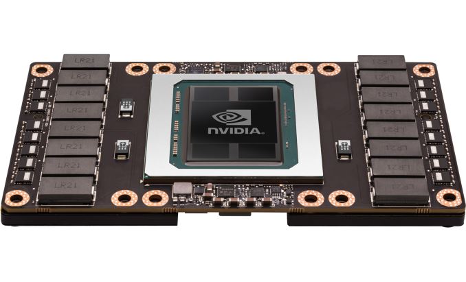
Today at their 2016 GPU Technology Conference, NVIDIA announced the first of their Pascal architecture powered Tesla cards, the Tesla P100. The P100 is the first major update to the Tesla HPC family since the launch of the first Kepler cards in late 2012, and represents a very sizable performance increase for the Tesla family thanks to the combination of the smaller 16nm manufacturing process and the Pascal architecture.
| NVIDIA Tesla Family Specification Comparison | ||||||
| Tesla P100 | Tesla K80 | Tesla K40 | Tesla M40 | |||
| Stream Processors | 3584 | 2 x 2496 | 2880 | 3072 | ||
| Core Clock | 1328MHz | 562MHz | 745MHz | 948MHz | ||
| Boost Clock(s) | 1480MHz | 875MHz | 810MHz, 875MHz | 1114MHz | ||
| Memory Clock | 1.4Gbps HBM2 | 5Gbps GDDR5 | 6Gbps GDDR5 | 6Gbps GDDR5 | ||
| Memory Bus Width | 4096-bit | 2 x 384-bit | 384-bit | 384-bit | ||
| Memory Bandwidth | 720GB/sec | 2 x 240GB/sec | 288GB/sec | 288GB/sec | ||
| VRAM | 16GB | 2 x 12GB | 12GB | 12GB | ||
| Half Precision | 21.2 TFLOPS | 8.74 TFLOPS | 4.29 TFLOPS | 6.8 TFLOPS | ||
| Single Precision | 10.6 TFLOPS | 8.74 TFLOPS | 4.29 TFLOPS | 6.8 TFLOPS | ||
| Double Precision | 5.3 TFLOPS (1/2 rate) |
2.91 TFLOPS (1/3 rate) |
1.43 TFLOPS (1/3 rate) |
213 GFLOPS (1/32 rate) |
||
| GPU | GP100 (610mm2) |
GK210 | GK110B | GM200 | ||
| Transistor Count | 15.3B | 2 x 7.1B(?) | 7.1B | 8B | ||
| TDP | 300W | 300W | 235W | 250W | ||
| Cooling | N/A | Passive | Active/Passive | Passive | ||
| Manufacturing Process | TSMC 16nm FinFET | TSMC 28nm | TSMC 28nm | TSMC 28nm | ||
| Architecture | Pascal | Kepler | Kepler | Maxwell 2 | ||
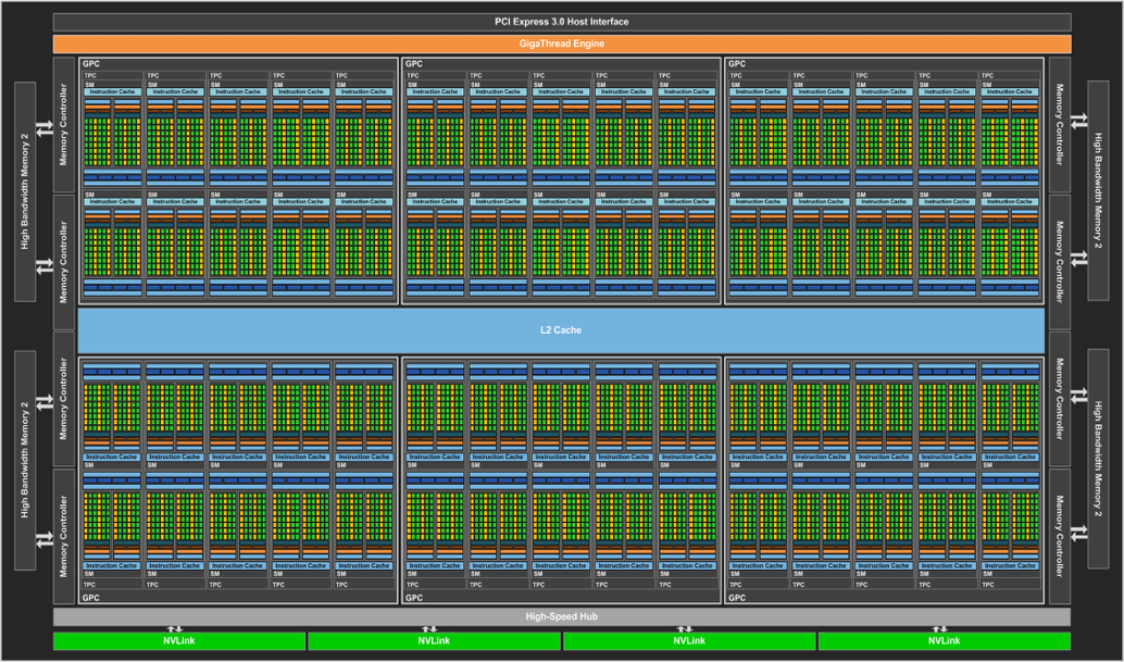
Powering the Tesla P100 is a partially disabled version of NVIDIA's new GP100 GPU, with 56 of 60 SMs enabled. GP100 is a whale of a GPU, measuring 610mm2 in die size on TSMC's 16nm FinFET process and composed of 15.3B transistors. It is remarkable in and of itself that NVIDIA and TSMC are in volume production of such a large 16nm die at this time, as everything else we've seen with a confirmed size is at best one-quarter of this size. GP100 is being produced on TSMC's Chip-On-Wafer-On-Substrate technology, with this line apparently being used for putting the GPU and HBM2 DRAM stacks on the same interposer.
We'll dive into the full Pascal architecture (as implemented by GP100) at a later time, but it's worth noting that Pascal here is 64 FP32 CUDA cores per SM, versus 128 on Maxwell. Each of those SMs also contains 32 FP64 CUDA cores - giving us the 1/2 rate for FP64 - and new to the Pascal architecture is the ability to pack 2 FP16 operations inside a single FP32 CUDA core under the right circumstances. With a boost clock of 1.48GHz, altogether Tesla P100 will offer 10.6 TFLOPS of FP32 performance or 5.3 TFLOPS of FP64 performance, more than doubling and tripling Tesla K40's rated throughput on these metrics respectively. NVIDIA has been happy to crow about the performance of Tesla P100, and for good reason, as this stands to be a very powerful processor.
Paired with the GP100 GPU on Tesla P100 is 16GB of HBM2 VRAM, laid out in 4 stacks for a 4096-bit memory bus. NVIDIA quotes P100 as offering 720GB/sec of memory bandwidth, which works out to a memory clock of 1.4Gbps. As we've seen with other HBM products, this marks a significant increase in memory bandwidth, more than doubling NVIDIA's last generation of cards.
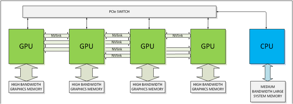
In their announcement, NVIDIA also confirmed that Tesla P100 will support NVLink, with 4 NVLink controllers. Previously announced, NVLink will allow GPUs to connect to either each other or to supporting CPUs (OpenPOWER), offering a higher bandwidth cache coherent link than what PCIe 3 offers. This link will be important for NVIDIA for a number of reasons, as their scalability and unified memory plans are built around its functionality.
Speaking of functionality, Tesla P100 and the underlying GP100 GPU is a full-featured HPC GPU. It supports all of the HPC-centric functionality that the Tesla K20/40/80 embodied, including ECC memory protection for the register file, caches, and HBM2 DRAM. Coupled with the very high FP64 rate, and it's clear that this is the successor of the GK110/GK210 GPU.

NVIDIA's pictures also confirm that this is using their new mezzanine connector, with flat boards no longer on perpendicular cards. This is a very HPC-centric design (I'd expect to see plenty of PCIe cards in time as well), but again was previously announced and is well suited for the market NVIDIA is going after, where these cards will be installed in a manner very similar to LGA CPUs. The P100 is rated for a TDP of 300W, so the cooling requirements are a bit higher than last-generation cards, most of which were in the 230W-250W range.
Finally, in its initial implementation NVIDIA is focusing on customers that need extreme scaling capabilities, and I wouldn't be too surprised if this was in part due to the margins of that market and how these initial cards will be in demand. NVLink of course plays a big part here, with NVIDIA able to go up to 8-way configurations thanks to it.


Source: NVIDIA


93 Comments
View All Comments
SunnyNW - Wednesday, April 6, 2016 - link
Please excuse the ignorance, but there are 3584 Stream Processors of the FP32 variety correct? So does that mean that the FP64 CUDA Cores per SM are separate hardware-wise and therefore there are 1792 of those on chip? Also could FP64 cores, theoretically, be used for games either by having them crunch 32bit math or however else?SunnyNW - Wednesday, April 6, 2016 - link
LOL, let me just say sorry Ryan. That is my younger brother asking that question since he finds it easier to use my login than to take the minuscule amount of time to sign-up for his own. It might explain some previous comments/questions too not sure how far back tho, not that I think its a big deal. Sorry, n its just funny on a personal level because he definitely does not talk like that or type like that from what I have seen haha. He's a pretty bright kid n Im glad he enjoys the workings of tech.But his last question does seem intriguing. I'm not sure if it would take some architecture changes (maybe?) but could FP64 cores be used in conjunction with FP32 cores to crunch the same type of dataset ("gaming" data). Is the gpu designed so that you are either using the 3584 FP32 cores OR the FP64 cores but not both at the same time? Could this just be as simple as being a power or thermal limit (running ALL the cores at the same time being too power hungry)?
extide - Tuesday, April 5, 2016 - link
Not sure what you are asking, but yes this is "Big Pascal" although they are currently only able to sell partially disabled versions because of the defect rate in the 16nm process.Samus - Wednesday, April 6, 2016 - link
Considering how functional the die is (over 90%) yields appear surprisingly good. They might have a fully enabled die to market in a year, if there is even any competition to push them to do so. Here's hoping AMD pulls off something good.jasonelmore - Tuesday, April 5, 2016 - link
not much more because they are already pushing the boundaries on die size.. unless they are counting the HBM in those figures, or they are counting multiple layers.Krysto - Tuesday, April 5, 2016 - link
Didn't they promise up to 32GB HBM2 GPUs, though?T1beriu - Tuesday, April 5, 2016 - link
You read so many made-up "leaks" that you started to believe them. :)prtskg - Wednesday, April 6, 2016 - link
It'll come later.extide - Tuesday, April 5, 2016 - link
Also, to add, GTX 1080 will probably be GP104. GP100 may end up in a GTX 1080 Ti, in a partially disabled form, and then probably also in a future Titan successor (possibly called Summit).ddriver - Tuesday, April 5, 2016 - link
Fat chance. It will not be the same chip, even the titans are crippled in terms of FP64