The Intel Xeon E5 v4 Review: Testing Broadwell-EP With Demanding Server Workloads
by Johan De Gelas on March 31, 2016 12:30 PM EST- Posted in
- CPUs
- Intel
- Xeon
- Enterprise
- Enterprise CPUs
- Broadwell
SAP S&D
The SAP S&D 2-Tier benchmark has always been one of my favorites. This is probably the most real world benchmark of all the server benchmarks done by the vendors. It is a full-blown application living on top of a heavy relational database. And don't forget that SAP is one of the most successful software companies out there, the market leader of Enterprise Resource Planning.
We analyzed the SAP Benchmark in-depth in one of our earlier articles:
- Very parallel resulting in excellent scaling
- Low to medium IPC, mostly due to "branchy" code
- Somewhat limited by memory bandwidth
- Likes large caches (memory latency)
- Very sensitive to sync ("cache coherency") latency
Let us see how the new Xeon E5 fares in this ERP benchmark.
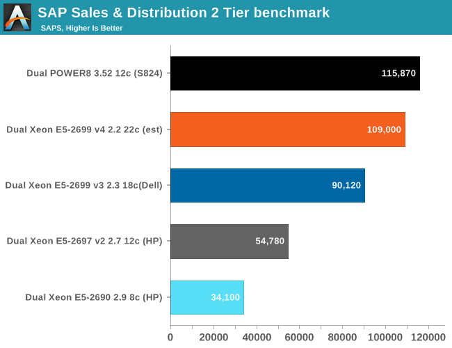
(est) = Preliminary data
The ever-increasing L3 cache, high core counts, and better NUMA coherency support of Broadwell-EP play well with SAP. It is almost like Intel builds these Xeons for SAP alone. The result is that the current Xeon is no less than 3 times faster than the Xeon 2690 (v1).


112 Comments
View All Comments
Kevin G - Thursday, March 31, 2016 - link
Much like how Apple skipped Haswell-EP, they also skipped a generation of cards from AMD and nVidia. So even if Apple doesn't wait for new GPUs, their is certainly an update on the GPU side.The more interesting possibility would be if Apple were to go with Xeon D in the Mac Pro instead of Broadwell-EP. Apple would need a big PLX chip considering the number of lanes they's want to use but it is possible.
bill.rookard - Thursday, March 31, 2016 - link
Another issue is that they're not under any pressure from any competition to really innovate. I don't even remember the last time I read anything about Opteron servers... let alone something about any NEW Opterons.ComputerGuy2006 - Thursday, March 31, 2016 - link
A sign of things to come for Broadwell-e?Seems like a tricky situation. Because skylake-e will come with a new platform in 2017, while broadwell-e isn't the fastest IPC and there are crazy rumors it will might cost $1500 (lol Intel). We also have Zen later this year that might give good performance with good cost/perf ratio.
extide - Thursday, March 31, 2016 - link
Yeah so Intel only gives us the LCC part for the -E platform, so we will see the 10-core SKU as the top, It will either be $1000, or $1500 ... so yeah not sure how that will end up. Although there will be 8 and 6 core options that should be pretty affordable.Hopefully they do an 8 core part with 28 lanes for under $500, as THAT would be a great deal!
dragonsqrrl - Sunday, April 3, 2016 - link
I'm hoping the 8 core SKU is around $600, the position the x930K traditionally occupies. What makes me a little worried is that there will be 4 SKUs instead of 3 this time (one 10 core, one 8 core, and two 6 core), and I'm not sure there's enough room under the $600 price point for two 6 core processors.jasonelmore - Thursday, March 31, 2016 - link
Can it run Star Citizen?theduckofdeath - Thursday, March 31, 2016 - link
A question we'll never get an answer to? :DJohanAnandtech - Friday, April 1, 2016 - link
It probably runs mostly on Xeons. Well, the back end that is :-)extide - Thursday, March 31, 2016 - link
BOOM, 454mm^2 on the worlds best process. The "other" 14/16nm processes use bigger geometry than Intel's 14nm process.Now we just need those other guys to catch up so we can see 450+mm GPU's!
Kevin G - Thursday, March 31, 2016 - link
Intel still has plenty of room to increase die size. The largest chip they've produced was the Tukwila Itanium 2 at 699 mm^2. Granted that was a 65 nm design but Haswell-EX is a juggarnaught at 662 mm^2 on Intel's more recent 22 nm process. Seems reasonable that SkyLake-EX could go to 32 cores as Intel has >200 mm^2 of rectal limit left.As for GPU's, they're also huge. nVidia's GM200 is 601 mm^2 and AMD's Fiji is 'only' 596 mm^2 both on 28 nm process. TSMC's 20 nm process was skipped so even using the looser 16 nm FinFET, GPU's will see a significant shrink compared to the those high end chips.