TSMC

TSMC's 3D-stacked system-on-integrated chips (SoIC) advanced packaging technologies is set to evolve rapidly. In a presentation at the company's recent technology symposium, TSMC outlined a roadmap that will take the technology from a current bump pitch of 9μm all the way down to a 3μm pitch by 2027, stacking together combinations of A16 and N2 dies. TSMC has a number of advanced packaging technologies, including 2.5D CoWoS and 2.5D/3D InFO. Perhaps the most intriguing (and complex) method is their 3D-stacked system-on-integrated chips (SoIC) technology, which is TSMC's implementation of hybrid wafer bonding. Hybrid bonding allows two advanced logic devices to be stacked directly on top of each other, allowing for ultra-dense (and ultra-short) connections between the two chips, and is primarily aimed at high performance...
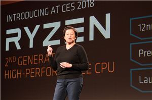
Getting Radeon Vega Everywhere: An Exclusive Media Interview at AMD Tech Day, with CEO Dr. Lisa Su
In what is becoming an annual tradition, during AMD’s Tech Day here at CES we were given the opportunity to spend some time with Dr. Lisa Su, AMD’s CEO...
65 by Ian Cutress on 1/24/2018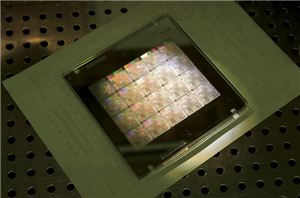
TSMC Teams Up with ARM and Cadence to Build 7nm Data Center Test Chips in Q1 2018
TSMC has announced plans to build its first test chips for data center applications using its 7 nm fabrication technology. The chip will use compute cores from ARM, a...
12 by Anton Shilov on 9/14/2017
Microsoft’s Project Scorpio: More Hardware Details Revealed
This news piece contains speculation, and suggests silicon implementation based on released products and roadmaps. The only elements confirmed for Project Scorpio are the eight x86 cores, 6 TFLOPs...
113 by Ian Cutress on 4/6/2017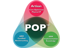
ARM Announces 10FF "Artemis" Test Chip
Today in collaboration with TSMC, ARM's physical IP division is announcing the tapeout of a 10nm test chip demonstrating the company's readiness for the new manufacturing process. The new...
24 by Andrei Frumusanu on 5/18/2016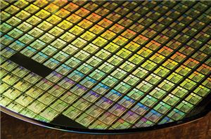
EUV Lithography Makes Good Progress, Still Not Ready for Prime Time
At the recent annual SPIE Advanced Lithography conference, Intel, TSMC and other leading semiconductor companies said that significant strides have been made in extreme ultraviolet lithography (EUVL) over the...
38 by Anton Shilov on 3/10/2016


