Google's Tensor inside of Pixel 6, Pixel 6 Pro: A Look into Performance & Efficiency
by Andrei Frumusanu on November 2, 2021 8:00 AM EST- Posted in
- Mobile
- Smartphones
- SoCs
- Pixel 6
- Pixel 6 Pro
- Google Tensor
Google's IP: Tensor TPU/NPU
At the heart of the Google Tensor, we find the TPU which actually gives the chip is marketing name. Developed by Google with input and feedback by the team’s research teams, taking advantage of years of extensive experience in the field of machine learning, Google puts a lot of value into the experiences that the new TPU allows for Pixel 6 phones. There’s a lot to talk about here, but let’s first try to break down some numbers, to try to see where the performance of the Tensor ends up relative to the competition.
We start off with MLCommon’s MLPerf – the benchmark suite works closely with all industry vendors in designing something that is representative of actual workloads that run on devices. We also run variants of the benchmark which are able to take advantage of various vendors SDKs and acceleration frameworks. Google had sent us a variant of the MLPerf app to test the Pixel 6 phones with – it’s to be noted that the workloads on the Tensor run via NNAPI, while other phones are optimised to run through the respective chip vendor’s libraries, such as Qualcomm’s SNPE, Samsung’s EDEN, or MediaTek’s Neuron – unfortunately only the Apple variant is lacking CoreML acceleration, thus we should expect lower scores on the A15.
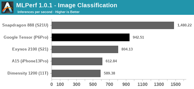
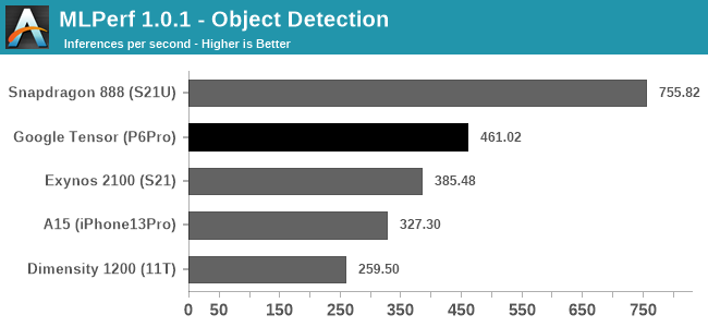
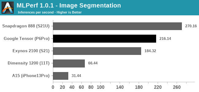
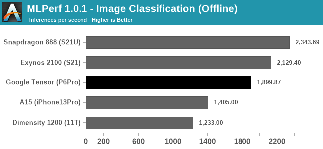
Starting off with the Image Classification, Object Detection, and Image Segmentation workloads, the Pixel 6 Pro and the Google Tensor showcase good performance, and the phone is able to outperform the Exynos 2100’s NPU and software stack. More recently, Qualcomm had optimised its software implementation for MLPerf 1.1, able to achieve higher scores than a few months ago, and this allows the Snapdragon 888 to achieve significantly better scores than what we’re seeing on the Google Tensor and the TPU – at least for those workloads, in the current software releases and optimisations.
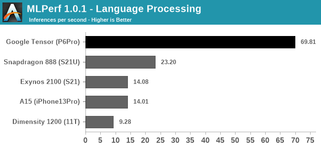
The Language Processing test of MLPerf is a MobileBERT model, and here for either architectural reasons of the TPU, or just a vastly superior software implementation, the Google Tensor is able to obliterate the competition in terms of inference speed.
In Google’s marketing, language processing, such as live transcribing, and live translations, are very major parts of the differentiating features that the new Google Tensor enables for the Pixel 6 series devices – in fact, when talking about the TPU performance, it’s exactly these workloads that the company highlights as being the killer use-cases and what the company calls state-of-the-art.
If the scores here are indeed a direct representation of Google’s design focus of the TPU, then that’s a massively impressive competitive advantage over other platforms, as it represents a giant leap in performance.
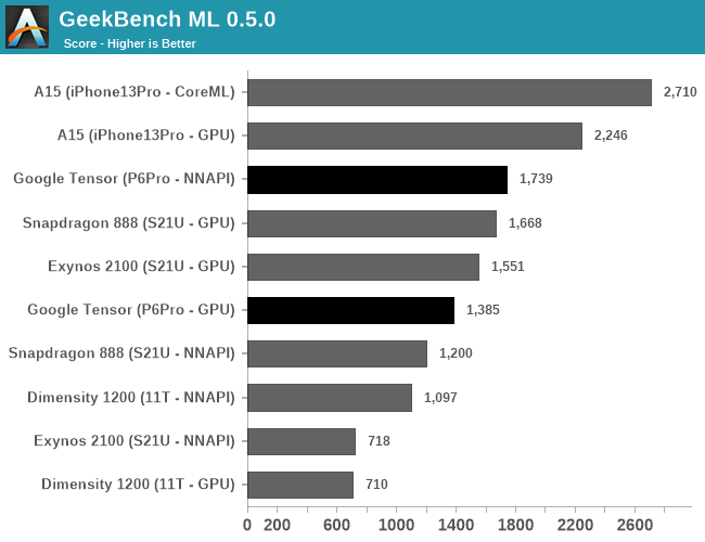
Other benchmarks we have available are for example GeekBench ML, which is currently still in a pre-release state in that the models and acceleration can still change in further updates.
The performance here depends on the APIs used, with the test either allowing TensorFlow delegates for the GPU or CPU, or using NNAPI on Android devices (and CoreML on iOS). The GPU results should only represent the GPU ML performance, which is surprisingly not that great on the Tensor, as it somehow lands below the Exynos 2100’s GPU.
In NNAPI mode, the Tensor is able to more clearly distinguish itself from the other SoCs, showcasing a 44% lead over the Snapdragon 888. It’s likely this represent the TPU performance lead, however it’s very hard to come to conclusions when it comes to such abstractions layer APIs.
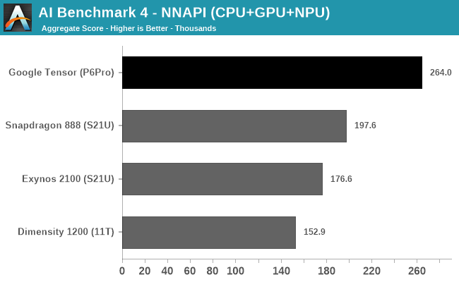
In AI Benchmark 4, when running the benchmark in pure NNAPI mode, the Google Tensor again showcases a very large performance advantage over the competition. Again, it’s hard to come to conclusions as to what’s driving the performance here as there’s use of CPU, GPU, and NPUs.
I briefly looked at the power profile of the Pixel 6 Pro when running the test, and it showcased similar power figures to the Exynos 2100, which extremely high burst power figures of up to 14W when doing individual inferences. Due to the much higher performance the Tensor showcases, it also means it’s that much more efficient. The Snapdragon 888 peaked around 12W in the same workloads, so the efficiency gap here isn’t as large, however it’s still in favour of Google’s chip.
All in all, Google’s ML performance of the Tensor has been its main marketing point, and Google doesn’t disappoint in that regard, as the chip and the TPU seemingly are able to showcase extremely large performance advantages over the competition. While power is still very high, completing an inference faster means that energy efficiency is also much better.
I asked Google what their plans are in regards to the software side of things for the TPU – whether they’ll be releasing a public SDK for developers to tap into the TPU, or whether things will remain more NNAPI centric like how they are today on the Pixels. The company wouldn’t commit yet to any plans as it’s still very early – in generally that’s the same tone we’ve heard from other companies as even Samsung, even 2 years after the release of their first-gen NPU, doesn’t publicly make available their Eden SDK. Google notes that there is massive performance potential for the TPU and that the Pixel 6 phones are able to use them in first-party software, which enables the many ML features for the camera, and many translation features on the phone.


108 Comments
View All Comments
Speedfriend - Thursday, November 4, 2021 - link
The average laptop costs $500 and most expensive laptops are bought by enterprises where Mac OS has a limited share. While the Macbookz are great devices, they are hobbled by poor monitor support at the Air end and cray prices at the MacBook Pro end. For most users the difference between the performance of a MacBook Pro and a $1000 laptop is unnoticeable except in their wallet!dukhawk - Tuesday, November 2, 2021 - link
The chip is very Exynos design related. Looking through the kernel source and there are a ton of Exynos named files.dukhawk - Tuesday, November 2, 2021 - link
https://android.googlesource.com/device/google/rav...defaultluser - Tuesday, November 2, 2021 - link
If anyone wants to know know why Nvidia is most interested in purchasing ARM, it's in order to put the inefficient Mali out of it's misery - and simultaneously replace it with their own license-able Geforce cores!Since ARM Corp started throwing in the GPU for free, they've had to cut GPU research (to pay for the increasingly complex CPU cores, all of which come out of the same revenue box!) But Nvidia has the massive Server Revenue to handle this architecture-design mismatch; they will keep the top 50% of the engineers, and cut the other cruft loose!
melgross - Tuesday, November 2, 2021 - link
That may be a side effect. But the reason for purchasing g it would be maki g money, and controlling the market. Yes, it’s true that Nvidia wa t to control all graphics and to turn the GPU into the main programming aim.TheinsanegamerN - Tuesday, November 2, 2021 - link
If nvidia wanted to do that they could simply license ARM and make their own superior chip. The fact they have fallen flat on their face every time they have tried speaks volumes.they want ARM for patents and $$$, nothing more.
defaultluser - Wednesday, November 3, 2021 - link
When a place like Rockchip can sell an Arm chip bundled with Mali for Peanuts, you can understand why superior GPU wasn't enough to win Phone customers!You also need integrated modem if you ever want to compete with Qualcomm (not something Nvidia was willing to do).
But that bundling system has been shorting ARM Mali development for years (Qualcomm, Apple, and soon Samsung (via AMD) are all bringing better high-end options into the field - you know your performance/watt must be pathetic when a company like Samsung is getting desperate-enough to pay the cost of porting AMD GPU over to ARM architecture.
Kvaern1 - Sunday, November 7, 2021 - link
"If nvidia wanted to do that they could simply license ARM and make their own superior chip."''simply'
No, no one can simply do that anymore and only two companies can. NVidia just bought one of them.
melgross - Tuesday, November 2, 2021 - link
I’m wondering about several things here.I don’t see the reason for using the A76 cores being one of time. This is a very new chip. The competitors on the Android side have been out for a while. They use A78 cores. Samsung uses A78 cores. So time doesn’t seem to be the issuer here, after all it does use the X1. So I wonder if it isn’t the size of the core on this already large, crowded chip that’s a reason, and possibly cost. If the newer cores take up more area they would cost slightly more. These chips are going to be bought in a fairly small number. Estimates have it that last year, Google sold between 4 and 7 million phones, and that they’re doubling this year’s order. Either would still be small, and give no advantage to Google in volume pricing compared to other chip makers.
The second is that you have to wonder if Google is following the Apple road here. Apple, of course, designs many chips, all for their own use. Will Google keep their chips for their own use, assuming they’re as successful in selling phones as Google hopes, or will they, after another generation, or two, when the chip is more of their own IP, offer them to other Android phone makers, and if so, how will Samsung feel about that, assuming their contract allows it?
SonOfKratos - Tuesday, November 2, 2021 - link
I think they went for the A76 cores because of cost, like you said Tensor is already huge and the A78 or A77 cores would be more power efficient but they are also much bigger than the A76 on 5nm process. Even if they were to clock an A78 lower it would just be a waste of money and space on the chip for them. They probably had a specific budget for the chip which meant a specific die size. This is not Apple who is willing to throw as much money as they can to get the best performance per watt.The display was rumored to be an E5 display from Samsung display which is in their latest display so I don't know why Google is not pushing for higher brightness but it could be because of heat dissipation as well...I highly doubt Samsung gave Google their garbage displays lol Also Google does not utilize the variable refresh rate very well and it's terrible for battery life. I have also seen a lot of janky scrolling with 120Hz in apps like Twitter..it has hiccups scrolling through the timeline compared to my Pixel 3.
The modem is very interesting probably more so than Tensor, this is the first competition for Qualcomm in the US at least. A lot of people have been saying that the modem is integrated in Tensor but why would Google integrate a modem that does not belong to them in "their" chip? That's like asking Apple to integrate Qualcomm modems in their chip. Also Samsung pays Qualcomm royalties for 5G so they probably have a special agreement surrounding the sale and implementation of the modem. It is definitely not as power efficient as Qualcomm's implementation but it's Good start. I got 400+ Mbps on T-Mobile 5GUC outdoors and 200 Mbps indoors (I don't know which band). It surprisingly supports n258 band like the iPhone.