The Apple iPhone 11, 11 Pro & 11 Pro Max Review: Performance, Battery, & Camera Elevated
by Andrei Frumusanu on October 16, 2019 8:30 AM ESTThe Apple A13 SoC: Lightning & Thunder
Apple’s A13 SoC is the newest iteration in the company’s silicon design efforts. The new silicon piece is manufactured on what Apple calls a “second generation 7nm manufacturing process”. The wording is a bit ambiguous, however, as it’s been repeatedly pointed out that this would mean TSMC’s N7P node, which is a performance tuned variant of last year’s N7 node, and not the N7+ node which is based on EUV production.
Update October 27th: TechInsights has now officially released a die shot of the new Apple A13, and we can confirm a few assumptions on our side.
The new die is 98.48mm² which is 18.3% larger than the A12 of last year. Given that this year’s manufacturing node hasn’t seen any major changes in terms of process density, it’s natural for the die size to increase a bit as Apple adds more functionality to the SoC.
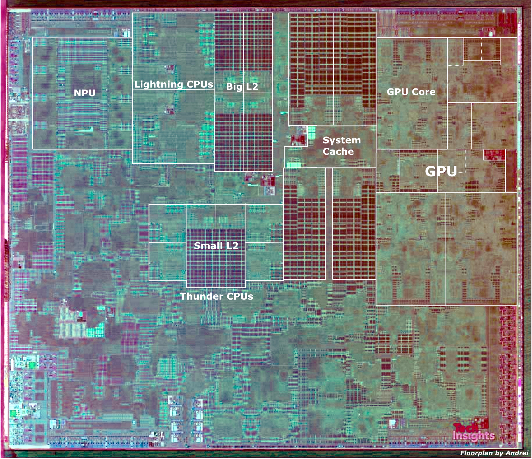
AnandTech modified TechInsights Apple A13 Die Shot
| Die Block Comparison (mm²) | ||
| SoC Process Node |
Apple A13 TSMC N7P |
Apple A12 TSMC N7 |
| Total Die | 98.48 | 83.27 |
| Big Core | 2.61 | 2.07 |
| Small Core | 0.58 | 0.43 |
| CPU Complex (Cores & L2) |
13.47 (9.06 + 4.41) |
11.16 (8.06 + 3.10) |
| GPU Total | 15.28 | 14.88 |
| GPU Core | 3.25 | 3.23 |
| NPU | 4.64 | 5.79 |
| SLC Slice (SRAM+Tag Logic) |
2.09 | 1.23 |
| SLC SRAM (All 4 Slices) |
6.36 | 3.20 |
When breaking down the block sizes of the different IP on the SoC, we can see some notable changes: The big new Lightning cores have increased in size by ~26% compared to last year, a large increase as we expect the new cores to have new functional units. The small Thunder cores have also increase in size by a massive 34% compared to last year’s Tempest cores, pointing out to the large microarchitecture changes we'll discuss in a bit.
The L2 on the big cores looks relatively similar to that of the A12, pointing out to a maintained 8MB size. What’s interesting is that the L2 of the small cores has now seen significantly changes, and the two slices that this cluster now embeds look quite identical to the slices of the large core's L2. It’s thus very likely that we’re looking at an increased 4MB of total L2 for the small Thunder cores.
The GPU footprint has slightly increased by a more marginal 3.8% - the biggest change seems to have been a rearrangement of the ALU blocks and texture unit layout of the GPU back-end, as the front-end blocks of the new IP looks largely similar to that of the A12.
The NPU has seen a large reduction in size and is now 20% smaller than that of the A12. As the A12’s NPU was Apple’s first in-house IP it seems natural for the company to quickly iterate and optimise on the second-generation design. It’s still a notably large block coming in at 4.64mm².
By far the biggest change on the SoC level has been the new system level cache (SLC). Already last year Apple had made huge changes to this block as it had adopted a new microarchitecture and increased the size from 4MB to 8MB. This year, Apple is doubling down on the SLC and it’s very evidently using a new 16MB configuration across the four slices. A single SLC slice without the central arbitration block increases by 69% - and the actual SRAM macros seen on the die shot essentially double from a total of 3.20mm² to 6.36mm².
The amount of SRAM that Apple puts on the A13 is staggering, especially on the CPU side: We’re seeing 8MB on the big cores, 4MB on the small cores, and 16MB on the SLC which can serve all IP blocks on the chip.
CPU Frequencies
The CPU complex remains a 2+4 architecture, supporting two large performance cores and four smaller efficiency cores. In terms of the frequencies of the various cores, we can unveil the following behavior changes to the A13:
| Maximum Frequency vs Loaded Threads Per-Core Maximum MHz |
||||||
| Apple A12 | 1 | 2 | 3 | 4 | 5 | 6 |
| Performance 1 | 2514 | 2380 | 2380 | 2380 | 2380 | 2380 |
| Performance 2 | 2380 | 2380 | 2380 | 2380 | 2380 | |
| Efficiency 1 | 1587 | 1562 | 1562 | 1538 | ||
| Efficiency 2 | 1562 | 1562 | 1538 | |||
| Efficiency 3 | 1562 | 1538 | ||||
| Efficiency 4 | 1538 | |||||
| Apple A13 | 1 | 2 | 3 | 4 | 5 | 6 |
| Performance 1 | 2666 | 2590 | 2590 | 2590 | 2590 | 2590 |
| Performance 2 | 2590 | 2590 | 2590 | 2590 | 2590 | |
| Efficiency 1 | 1728 | 1728 | 1728 | 1728 | ||
| Efficiency 2 | 1728 | 1728 | 1728 | |||
| Efficiency 3 | 1728 | 1728 | ||||
| Efficiency 4 | 1728 | |||||
The large performance cores this year see a roughly 6% increase in clockspeeds, bringing them up to around 2666MHz. Last year we estimated the A12 large cores to clock in at around 2500MHz, but the more exact figure as measured by performance counters seems to be 2514MHz. Similarly, the A13’s big core clock should be a few MHz above our estimated 2666MHz clock. Apple continues to quickly ramp down in frequency depending on how many large cores are active, and as such will max out at 2590MHz even on the lightest threads. I also noted that frequency will quickly ramp up and down depending on instruction mix and the load complexity on the core.
The small efficiency cores have seen a larger 8.8 – 12.3% clock boost, bringing them to up to ~1728MHz. This is a good boost, but what’s also important is that the small cores now don’t clock down when there’s more of them active.
The Lightning Performance CPU Cores: Minor Upgrades, Mystery of AMX
The large cores for this generation are called “Lightning” and are direct successors to last year’s Vortex microarchitecture. In terms of the core design, at least in regards to the usual execution units, we don’t see too much divergence from last year’s core. The microarchitecture at its heart is still a 7-wide decode front-end, paired with a very wide execution back-end that features 6 ALUs and three FP/vector pipelines.
Apple hasn’t made any substantial changes to the execution back-end, as both Lightning and Vortex are largely similar to each other. The notable exception to this is the complex integer pipelines, where we do see improvements. Here the two multiplier units are able to shave off one cycle of latency, dropping from 4 cycles to 3. Integer division has also seen a large upgrade as the throughput has now been doubled and latency/minimum number of cycles has been reduced from 8 to 7 cycles.
Another change in the integer units has been a 50% increase in the number of ALU units which can set condition flags; now 3 of the ALUs can do this, which is up from 2 in A12's Vortex.
As for the floating point and vector/SIMD pipelines, we haven't noticed any changes there.
In terms of caches, Apple seems to have kept the cache structures as they were in the Vortex cores of the A12. This means we have 8-way associative 128KB L1 instruction and data caches. The data cache remains very fast with a 3-cycle load-to-use latency. The shared L2 cache between the cores continues to be 8MB in size, however Apple has reduced the latency from 16 to 14 cycles, something we’ll be looking at in more detail on the next page when looking at the memory subsystem changes.
A big change to the CPU cores which we don’t have very much information on is Apple’s integration of “machine learning accelerators” into the microarchitecture. At heart these seem to be matrix-multiply units with DSP-like instructions, and Apple puts their performance at up to 1 Tera Operations (TOPs) of throughput, claiming an up-to 6x increase over the regular vector pipelines. This AMX instruction set is seemingly a superset of the ARM ISA that is running on the CPU cores.
There’s been a lot of confusion as to what this means, as until now it hadn’t been widely known that Arm architecture licensees were allowed to extend their ISA with custom instructions. We weren’t able to get any confirmation from either Apple or Arm on the matter, but one thing that is clear is that Apple isn’t publicly exposing these new instructions to developers, and they’re not included in Apple’s public compilers. We do know, however, that Apple internally does have compilers available for it, and libraries such as the Acclerate.framework seem to be able to take advantage of AMX. Unfortunately, I haven't had the time or experience to investigate this further for this article.
Arm’s recent reveal of making custom instructions available for vendors to implement and integrate into Arm’s cores certainly seems evidence enough that architecture licensees would be free to do what they’d like – Apple’s choice of hiding away AMX instructions at least resolves the concern about possible ISA fragmentation on the software side.
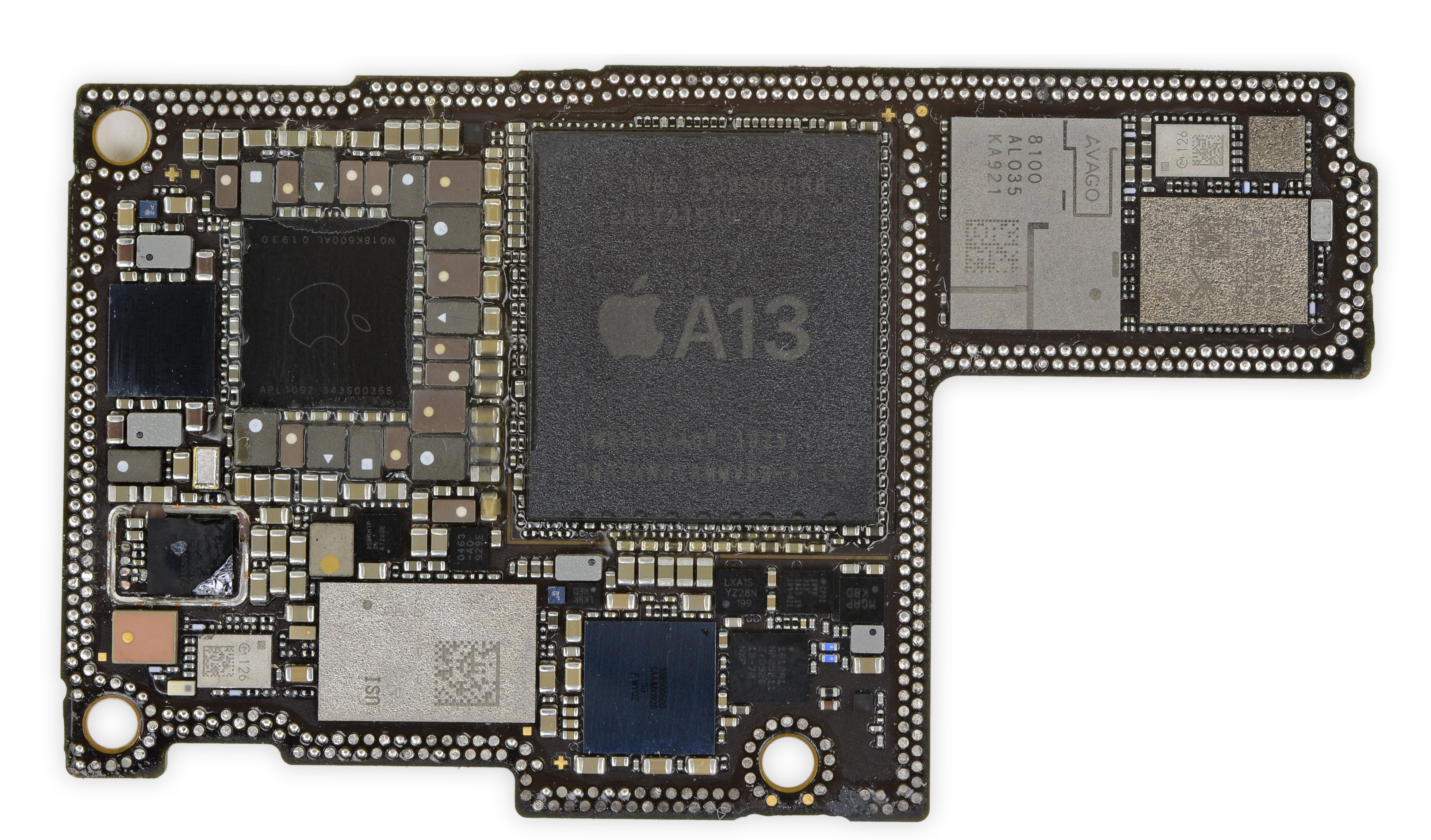
Apple's iPhone 11 Pro Max Motherboard with the A13 SoC (Image Courtesy iFixit)
The Thunder Efficiency CPU Cores: Major Upgrades
Apple’s small efficiency cores are extremely interesting because they’re not all that small when compared to the typical little cores from Arm, such as the Cortex-A55. Last year’s Tempest efficiency cores in the A12 were based on a 3-wide out-of-order microarchitecture with two main execution pipelines, working alongside L/S units and what we assume is a dedicated division unit.
This year’s Thunder microarchitecture seems to have made major changes to the efficiency CPU core, as we’re seeing substantial upgrades in the execution capabilities of the new cores. In terms of the integer ALUs we’re seemingly still looking at two units here, however Apple has doubled the number of units capable of flag set operations from 1 to 2. MUL throughput remains at 1 instruction per cycle, while the division unit is also seemingly unchanged.
What’s actually more impressive is that the floating point and vector pipelines were essentially doubled: FP addition throughput has gone from 1 to 2, while the latency has been reduced from 4 to 3. This is mirrored by vector addition capabilities, with a TP of 2 and a latency of 2. This doubling of throughput is extended throughout almost all instructions executed in the FP/SIMD pipelines, with the exceptions being some operations such as multiplications and division.
The FP division unit has seen a massive overhaul, as it’s seemingly now a totally new unit that’s now optimized for 64-bit operations, no longer halving its throughput when operating on double-precision numbers. DP latencies have been reduced from 19 to 10 cycles, while SP latency has gone down from 12 to 9 cycles. Vector DP division operations have even seen silly improvements such as 4x increase in throughput and 1/3rd the latency.
The Thunder cores are now served by a 48KB L1 data cache, which is an increase over the 32KB we’ve seen in previous generations of Apple’s efficiency cores. We haven’t been able to confirm the L1 instruction cache. There also seems to have been changes to the L2 cache of the efficiency cores, which we'll discuss on the following page.

Looking at the performance of the new A13 Thunder cores, we’re seeing that the new microarchitecture has increased its IPC significantly, with gains ranging from 19% in 403.gcc to 38% in 400.perlbench in SPECint, while floating point performance has also improved by an equally impressive 34-38% in non-memory bound SPECfp workloads.
In other areas we're seeing some performance regressions, and this is because Apple has changed the DVFS policies of the memory subsystem, leading to the efficiency cores being unable to trigger some of the memory controller's higher frequency performance states. This results in some of the odd results we are seeing, such as 470.lbm.
This causes a bit of an issue for our dedicated measurements of the cores in isolation: given a more realistic workload such as a 3D game where the GPU would have the memory run at faster speed, the performance of the Thunder cores should be higher than what we see showcased here. I’ll attempt to measure the peak performance of the cores when they’re not limited by memory in a future update as I think it should be very interesting.
The power efficiency of the new cores is also significantly better. Granted, some of these improvements will be due to the system memory not running as fast, but given that the cores still deliver 10-23% higher average performance in the SPEC suites, it’s still massively impressive that energy consumption has gone down by 25% on average as well – pointing to major efficiency gains.
In the face of the relatively conservative changes of the Lightning cores (other than AMX), the new Thunder cores seem like an outright massive change for the A13 and a major divergence from Apple’s past efficiency core microarchitectures. In the face-off against a Cortex-A55 implementation such as on the Snapdragon 855, the new Thunder cores represent a 2.5-3x performance lead while at the same time using less than half the energy.


242 Comments
View All Comments
ksec - Wednesday, October 16, 2019 - link
Well At least one article got it right on Anandtech. Last time Anton refers Apple A13 as 7nm EUV, along with an TSMC update mentioning it as well. Now we can finally settle Apple is using N7P.I think one of the reason for the higher power usage is the A13 was designed with 7nm EUV in mind, and was only later changed to N7P as 7nm EUV may not provide enough capacity for Apple.
I do wonder if we are going to see 5nm Apple SoC next year.
Ian Cutress - Wednesday, October 16, 2019 - link
Anton didn't realise 'N7P' and 'N7+ with EUV' were different processes - and that people were using P instead of + for some unknown reason. Up until a while ago, any time someone said 'second generation N7', it was always thought of as N7+. Now we're making them clarify.FreckledTrout - Wednesday, October 16, 2019 - link
It's TSMC's alphabet soup so who can blame him. They could make the node names a bit easier for people whom are not CPU process nerds.dennphill - Wednesday, October 16, 2019 - link
Apple! They just give you what THEY want to! Pretty disappointed in all their products. I finally gave in and got rid of my Goggle thinggie (worthless, really) and got a reconditioned iPhone 8+ a coouple of months ago. It is really (so here's my technical user review: "It's just...") OK. My wife, OTOH, has an SE - her second - and she really doesn't want anything bigger. EVER! (Listen to that, Apple!) Even the reported new 'tiny' 2020 5.4" iPhone is what she calls HUGE. Weekend project is replacing her iPhone 5 SE battery that's begun not to keep a charge.peevee - Wednesday, October 16, 2019 - link
Make your bets: will Apple switch to A13X in their MacBooks... Seems would be very prudent with an 8-core implementation.solipsism - Wednesday, October 16, 2019 - link
I have no doubt Apple will replace Intel with an ARM SoC, but I do not expect it to be beefed up A-series chip found in an iPhone. Just like all their in-house designed chips, I would expect it to be its own letter designation with considerably more memory bandwidth, access to PCIe, and other features that work well in a lower-end portables and desktops.Diogene7 - Wednesday, October 16, 2019 - link
I hope Apple intend to keep their future laptop ARM CPU low power enough to not require any active cooling : a fanless ARM mac laptop is well executed could have a lot of appeal to me !!!That the reason why at the moment, I am keeping an eye on Samsung Galaxy Book S / Microsoft Surface Pro X that are the 2 first fanless computers with ARM Qualcomm 8cx : if responsiveness is good enough (especially for web browsing, watching video, Microsoft office,...) then it would prove it is possible.
From there, I would be very happy that Apple do an always connected fanless Macbook Air with an ARM CPU, as otherwise I am considering buying a Qualcomm 8cx fanless laptop (if the reviews confirms that the performance are reasonable enough)
joms_us - Wednesday, October 16, 2019 - link
I like to have this as well, approx. 1 day battery able to do media consumption/productivity. At least the comparison so far is that it is better if not than Intel Core i5-8250UQuantumz0d - Thursday, October 17, 2019 - link
This mentality shift that Apple caused in consumers is the reason why Laptops got rolled over into thin anf light disposable garbage.All Intel BGA / AMD (both PGA and BGA) all have castrated TDP limits which forces throttling. And Apple shoved an 6C/8T into which they cant cool because they tried to cheat physics. And still after VRM fiasco they still put the 8C/16T into that anemic chassis people who are buying them deserve to be robbed off th e 60% drop in performance.
Dell shoved XPS with same i9 and it got rekted down. Surface ARM cannot run 64bit x86 code and iy can run the UWP garbage only.
Next the BGA hellhole that Apple dragged everyone into. First x86 macs had BGA processors. Seeing that Intel stopped PGA and started Ultrabook BS and killed off all MX and XM PGA from Haswell making BGA with cTDP mandatory and bins locked down. My Haswell CPU in Notebook maintains consistent 700 in CB R15. Not even 7700HQ does it when put in a TDP locked JUNK.
And next Soldered SSD in Macs paired with T2 chip. Anything goes bad Go to Apple. Battery soldered to Chassis. KB inherent design flaw. This stupid corporate only knows how to fleece and put junk and forced all companies passively into this thin and light garbage.
Forget PCIE NVME SSDs in RAID rhat chassis will melt and GPUs don't exist in Apple lala land because Muh AR ML Kit and all.
ARM cannot do Transcoding work. Period. And Image Processing like Autodesk won't run on garbage ARM GPUs need Nvidia chips with High BW GDDR6 or G5X. Apple cannot cool them in that chassis. They can't escape Physics. End of Story of this A series competing with x86 ISA and Intel/AMD.
Diogene7 - Thursday, October 17, 2019 - link
@joms_us : Yes, for applications compiled to work natively on ARM64, the performance of the app running a Windows computer with Qualcomm 8cx should be similar as the same x86-32bits app running on a Windows computer with Intel Core i5-8250U, but with the advantage of having much better battery life which is appealing to me as well :).Really looking forward to read reviews on Samsung Galaxy Book S and Microsoft Surface Pro X to see if they hold to the hype...