The Intel 6th Gen Skylake Review: Core i7-6700K and i5-6600K Tested
by Ian Cutress on August 5, 2015 8:00 AM ESTSkylake's iGPU: Intel Gen9
Both the Skylake processors here use Intel’s HD 530 graphics solution. When I first heard the name, alarm bells went off in my head with questions: why is the name different, has the architecture changed, and what does this mean fundamentally?
Not coming up with many details, we did the obvious thing – check what information comes directly out of the processor. Querying HD 530 via Intel's OpenCL driver reports a 24 EU design running at 1150 MHz. This is different than what GPU-Z indicates, which points to a 48 EU design instead, although GPU-Z is not often correct on newer graphics modules before launch day. We can confirm that this is a 24 EU design, and this most likely follows on from Intel’s 8th Generation graphics in the sense that we have a base GT2 design featuring three sub-slices of 8 EUs each.
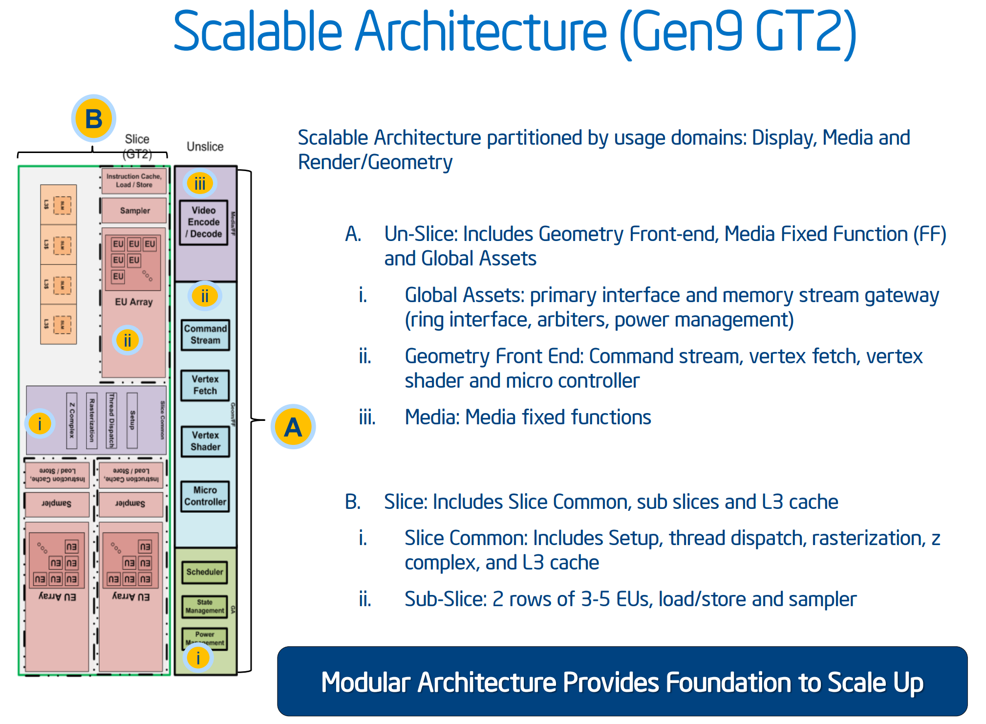
As far as we can tell, Intel calls the HD 530 graphics part of its 9th Generation (i.e. Gen9). We have been told directly by Intel that they have changed their graphics naming scheme from a four digit (e.g. HD4600) to a three digit (HD 530) arrangement in order "to minimize confusion" (direct quote). Personally we find that it adds more confusion, because the HD 4600 naming is not directly linked to the HD 530 naming. While you could argue that 5 is more than 4, but we already have HD 5200, HD 5500, Iris 6100 and others. So which is better, HD 530 or HD 5200? At this point it will already create a miasma of uncertainty, probably exaggerated until we get a definite explanation of the stack nomenclature.
Naming aside, Generation 9 graphics comes with some interesting enhancements. The slice and un-slice now have individual power and clock domains, allowing for a more efficient use of resources depending on the load (e.g. some un-slice not needed for some compute tasks). This lets the iGPU better balance power usage between fixed-function operation and programmable shaders.
Generation 9 will support a feature called Multi Plane Overlay, which is a similar feature to AMD’s video playback path adjustments in Carrizo. The principle here is that when a 3D engine has to perform certain operations to an image (blend, resize, scale), the data has to travel from the processor into DRAM then to the GPU to be worked on, then back out to DRAM before it hits the display controller, a small but potentially inefficient operation in mobile environments. What Multi Plane Overlay does is add fixed function hardware to the display controller to perform this without ever hitting the GPU, minimizing power consumption from the GPU and taking out a good portion of DRAM data transfers. This comes at a slight hit for die area overall due to the added fixed function units.
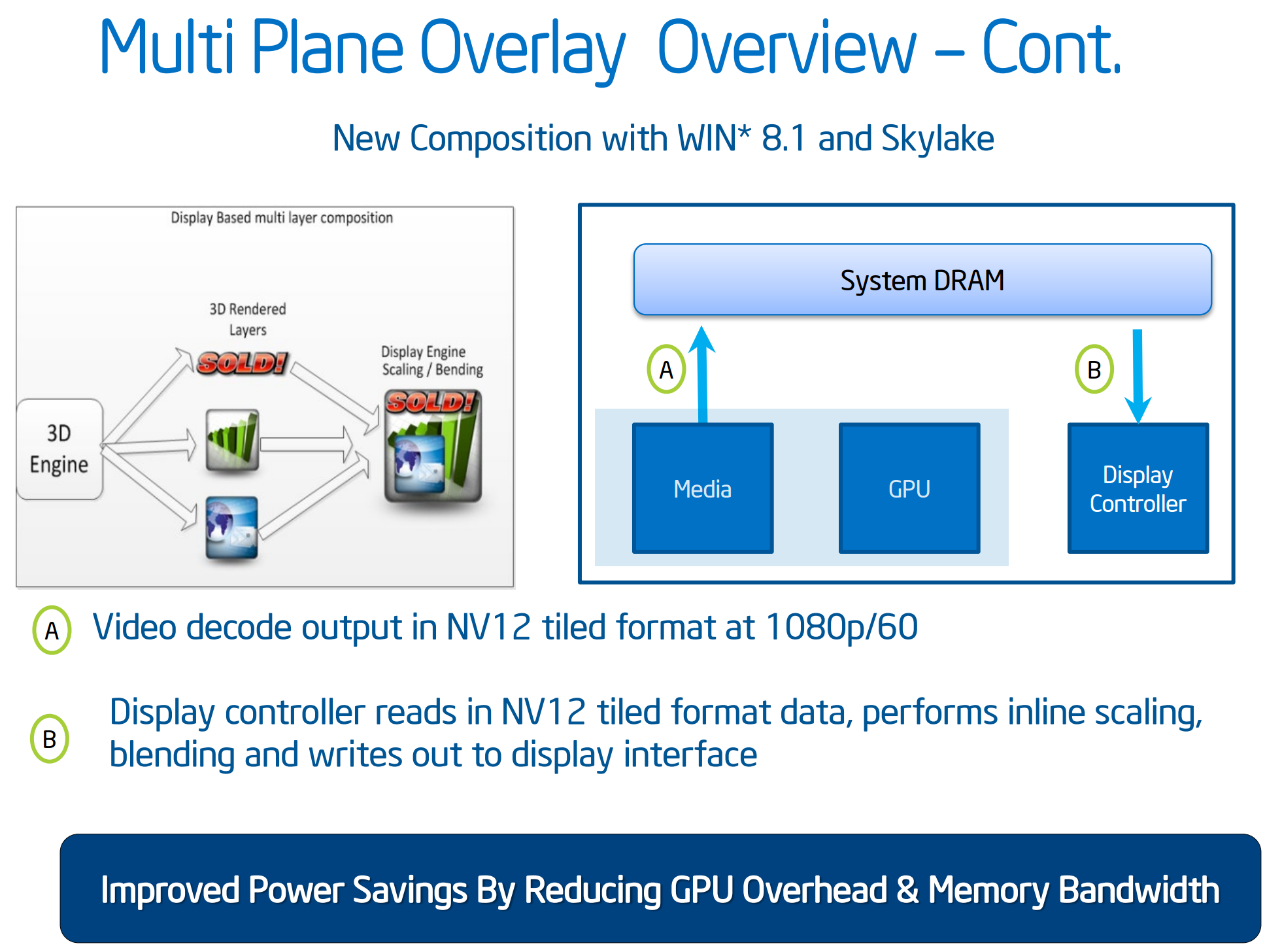
As shown above, this feature will be supported on Win 8.1 with Skylake’s integrated graphics. That being said, not all imaging can be moved in this way, but where possible the data will take the shorter path.
To go along with the reduced memory transfer, Gen9 has support for memory color stream compression. We have seen this technology come into play for other GPUs, where by virtue of fixed function hardware and lossless algorithms this means that smaller quantities of image and texture data is transferred around the system, again saving power and reducing bandwidth constraints. The memory compression is also used with a scalar and format conversion pipe to reduce the encoding pressure on the execution units, reducing power further.
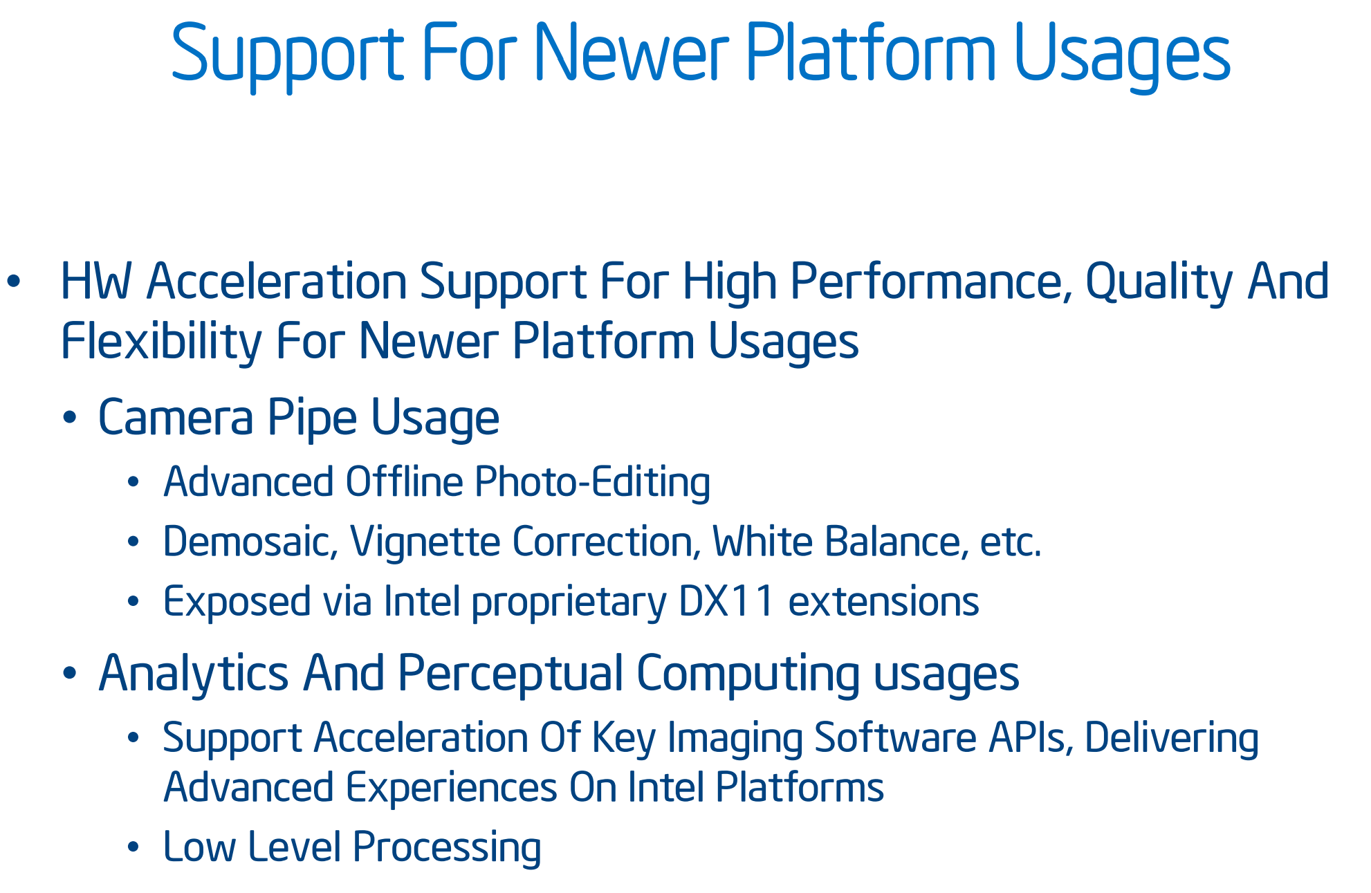
Adding into the mix, we have learned that Gen9 includes a feature called the ‘Camera Pipe’ for quick standard adjustments to images via hardware acceleration. This adjusts the programmable shaders to work in tandem for specific DX11 extensions on common image manipulation processes beyond resize/scale. The Camera Pipe is teamed with SDKs to help developers connect into optimized imaging APIs.
Media Encoding & Decoding
In the world of encode/decode, we get the following:
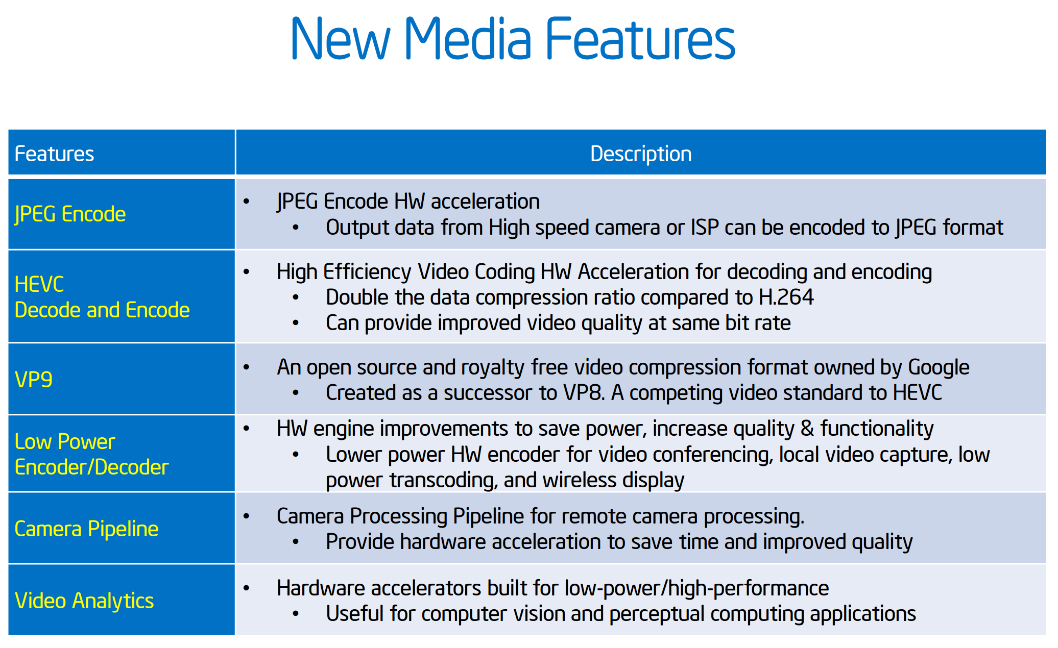
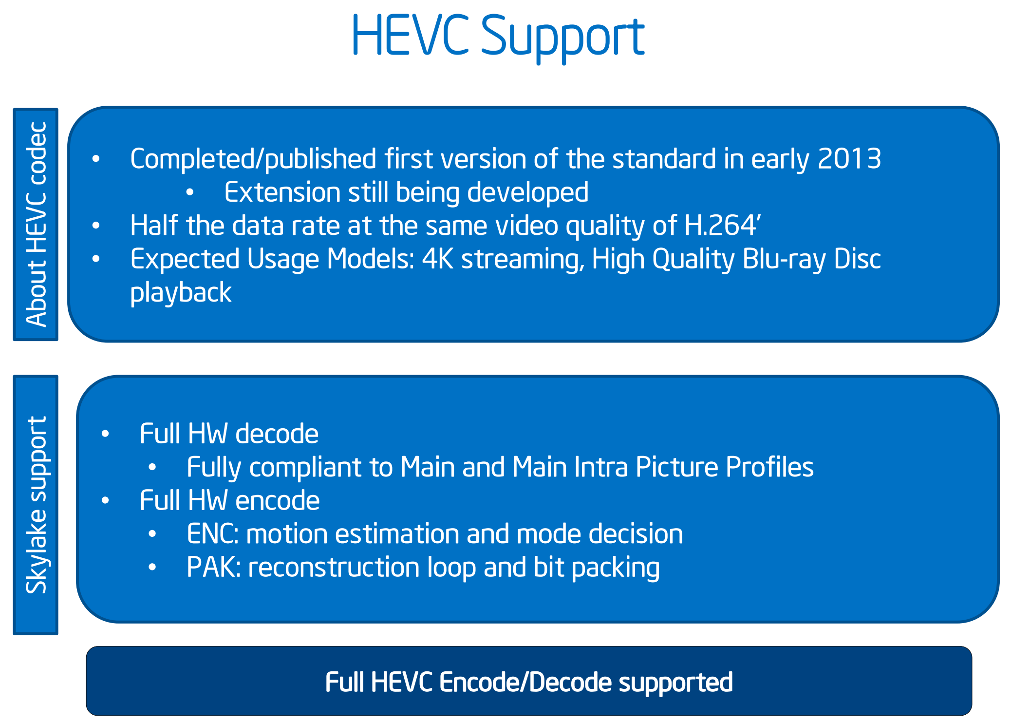
Whereas Broadwell implemented HEVC decoding in a "hybrid" fashion using a combination of CPU resources, GPU shaders, and existing GPU video decode blocks, Skylake gets a full, low power fixed function HEVC decoder. For desktop users this shouldn't impact things by too much - maybe improve compatibility a tad - but for mobile platforms this should significantly cut down on the amount of power consumed by HEVC decoding and increase the size and bitrate that the CPU can decode. Going hand-in-hand with HEVC decoding, HEVC encoding is now also an option with Intel's QuickSync encoder, allowing for quicker HEVC transcoding, or more likely real-time HEVC uses such as video conferencing.
Intel is also hedging their bets on HEVC by also implementing a degree of VP9 support on Skylake. VP9 is Google's HEVC alternative codec, with the company pushing it as a royalty-free option. Intel calls VP9 support on Skylake "partial" for both encoding and decoding, indicating that VP9 is likely being handled in a hybrid manner similar to how HEVC was handled on Broadwell.
Finally, JPEG encoding is new for Skylake and set to support images up to 16K*16K.
Video Support
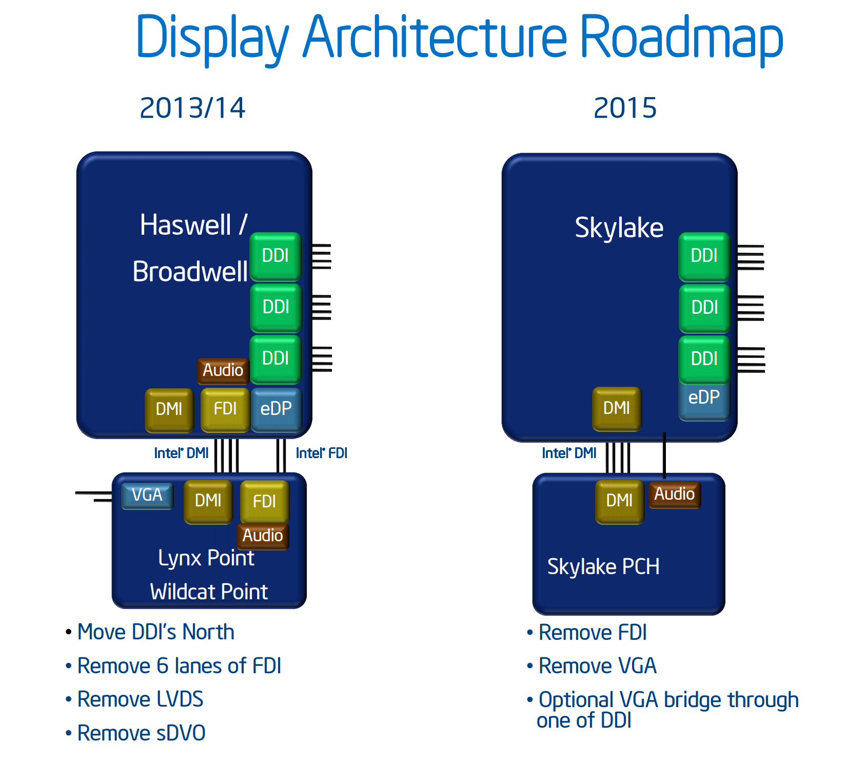
The analog (VGA) video connector has now been completely removed from the CPU/chipset combination, meaning that any VGA/D-Sub video connection has to be provided via an active digital/analog converter chip. This has been a long time coming, and is part of a previous committment made by Intel several years ago to remove VGA by 2015. Removing analog display functionality will mean added cost for legacy support in order to drive analog displays. Arguably this doesn’t mean much for Z170 as the high end platform is typically used with a discrete graphics card that has HDMI or DisplayPort, but we will see motherboards with VGA equipped in order to satisfy some regional markets with specific requirements.
HDMI 2.0 is not supported by default, and only the following resolutions are possible on the three digital display controllers:
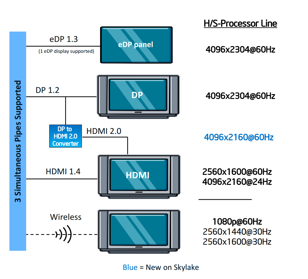
A DP to HDMI 2.0 converter, specifically an LS-Pcon, is required to do the adjustments, be it on the motherboard itself or as an external adapter. We suspect that there will not be many takers buying a controller to do this, given the capabilities and added benefits listed by the Alpine Ridge controller.


477 Comments
View All Comments
SuperVeloce - Saturday, August 8, 2015 - link
Wait, what? Skylake and 2011-3 in the same sentence? Who, for the love of god, would say such a thing? Power delivery is (again) new and very different from Haswell/Broadwell, so there is no chance to reuse 1150 and 2011-3Oxford Guy - Saturday, August 8, 2015 - link
The belief put forward was that Broadwell would be compatible with Haswell desktop motherboards and Skylake would be compatible with Haswell-E motherboards.KAlmquist - Saturday, August 8, 2015 - link
The analysis by Puget Sound Systems offers a plausible explanation of why Skylake has a higher TDP than Haswell or Ivy Bridge: the integrated GPU that comes with Skylake is faster and draws more power. It appears that if you don't use the integrated GPU, Skylake draws slightly less power than Haswell.SuperVeloce - Saturday, August 8, 2015 - link
That's definitely plausible. The other thing here is the TDP 4790K uses. 88W is too conservative for the clocks and voltages from that chip. They needed to up that I am sure.bobbozzo - Saturday, August 8, 2015 - link
Error in graph on final page:"Gains over Sandy Bridge.png" - the key for green says IVY bridge.
tuklap - Saturday, August 8, 2015 - link
I don't know... Intel seems to keep pushing forwards every year with profit in mind. The thing that they are really making breakthrough is the non volatile, high bandwidth memory or Xpoint...If Xpoint will be available maybe this will give a new speed bump... But Sandy-Skylake is really good...
wizyy - Saturday, August 8, 2015 - link
There is a review which shows 6600k to be quite a nice improvement over popular I5 processors in 10 recent games, over at eurogamer.net. Check it if you're a gamer thinking to upgrade your older I5.SilverManSachs - Saturday, August 8, 2015 - link
There is a good jump in IPC for the Core i5, less so for the Core i7. This makes sense as its harder to push the top end performance higher at smaller nodes but they did improve the i5 performance which is great as i5's are the most sold parts. Also, good overclocking room on the i7.Would be very interested to see 'Skylake vs Excavator' CPU only benchmarks on the mobile 17W parts. Please so that test for us AT!
soldier45 - Sunday, August 9, 2015 - link
Spending $500+ on Skylake over my 2600k to get 3-5 fps in my games isn't really worth it. Having said that at the end of the day,I'm about to spend $700 on a 980Ti over a 780 classified so yeh I will end up going with Skylake.asmian - Sunday, August 9, 2015 - link
The interesting fact for me faced with building a new rig is how the i7-6700K compares with the 28-lane Haswell-E i7-5820K. For my usage (design/programming, no interest in SLI/Crossfire, regular Handbrake use), with very comparable mid-range boards (ASRock Z170 Extreme6+ versus ASRock X99 Extreme4 with the USB 3.1 A/C card) the price of mobo + board is almost identical at £490 or so in the UK right now - in fact, the Haswell-E combo would be £15 cheaper. All other added components (DDR4 memory, new OS, M2 SSD etc.) would be identical.So do the extra 2 cores at a somewhat lower eventual overclock for that Handbrake usage make up for extremely marginal extra IPC on 4 cores at a higher price (and trading a few extra features for many less SATA ports)? Somehow I doubt it... The only question remaining would be whether waiting another year or more for Skylake-E would be worth it for even more chipset features over X99, but that looks rather marginal as well.