NVIDIA Tegra X1 Preview & Architecture Analysis
by Joshua Ho & Ryan Smith on January 5, 2015 1:00 AM EST- Posted in
- SoCs
- Arm
- Project Denver
- Mobile
- 20nm
- GPUs
- Tablets
- NVIDIA
- Cortex A57
- Tegra X1
GPU Performance Benchmarks
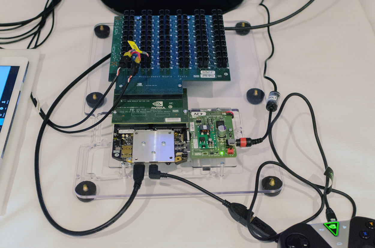
As part of today’s announcement of the Tegra X1, NVIDIA also gave us a short opportunity to benchmark the X1 reference platform under controlled circumstances. In this case NVIDIA had several reference platforms plugged in and running, pre-loaded with various benchmark applications. The reference platforms themselves had a simple heatspreader mounted on them, intended to replicate the ~5W heat dissipation capabilities of a tablet.
The purpose of this demonstration was two-fold. First to showcase that X1 was up and running and capable of NVIDIA’s promised features. The second reason was to showcase the strong GPU performance of the platform. Meanwhile NVIDIA also had an iPad Air 2 on hand for power testing, running Apple’s latest and greatest SoC, the A8X. NVIDIA has made it clear that they consider Apple the SoC manufacturer to beat right now, as A8X’s PowerVR GX6850 GPU is the fastest among the currently shipping SoCs.
It goes without saying that the results should be taken with an appropriate grain of salt until we can get Tegra X1 back to our labs. However we have seen all of the testing first-hand and as best as we can tell NVIDIA’s tests were sincere.
| NVIDIA Tegra X1 Controlled Benchmarks | |||||
| Benchmark | A8X (AT) | K1 (AT) | X1 (NV) | ||
| BaseMark X 1.1 Dunes (Offscreen) | 40.2fps | 36.3fps | 56.9fps | ||
| 3DMark 1.2 Unlimited (Graphics Score) | 31781 | 36688 | 58448 | ||
| GFXBench 3.0 Manhattan 1080p (Offscreen) | 32.6fps | 31.7fps | 63.6fps | ||
For benchmarking NVIDIA had BaseMark X 1.1, 3DMark Unlimited 1.2 and GFXBench 3.0 up and running. Our X1 numbers come from the benchmarks we ran as part of NVIDIA’s controlled test, meanwhile the A8X and K1 numbers come from our Mobile Bench.
NVIDIA’s stated goal with X1 is to (roughly) double K1’s GPU performance, and while these controlled benchmarks for the most part don’t make it quite that far, X1 is still a significant improvement over K1. NVIDIA does meet their goal under Manhattan, where performance is almost exactly doubled, meanwhile 3DMark and BaseMark X increased by 59% and 56% respectively.
Finally, for power testing NVIDIA had an X1 reference platform and an iPad Air 2 rigged to measure the power consumption from the devices’ respective GPU power rails. The purpose of this test was to showcase that thanks to X1’s energy optimizations that X1 is capable of delivering the same GPU performance as the A8X GPU while drawing significantly less power; in other words that X1’s GPU is more efficient than A8X’s GX6850. Now to be clear here these are just GPU power measurements and not total platform power measurements, so this won’t account for CPU differences (e.g. A57 versus Enhanced Cyclone) or the power impact of LPDDR4.
Top: Tegra X1 Reference Platform. Bottom: iPad Air 2
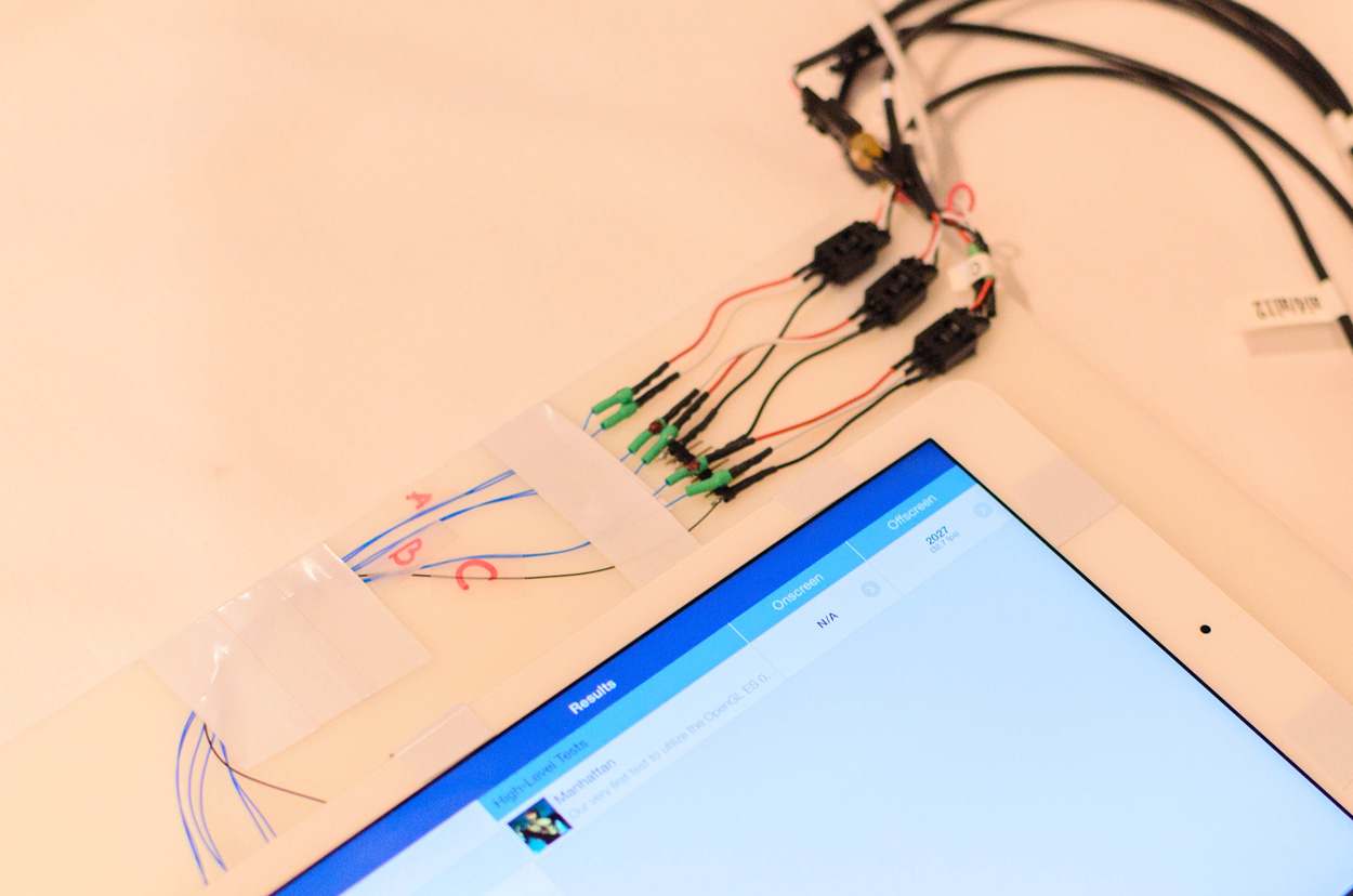
For power testing NVIDIA ran Manhattan 1080p (offscreen) with X1’s GPU underclocked to match the performance of the A8X at roughly 33fps. Pictured below are the average power consumption (in watts) for the X1 and A8X respectively.
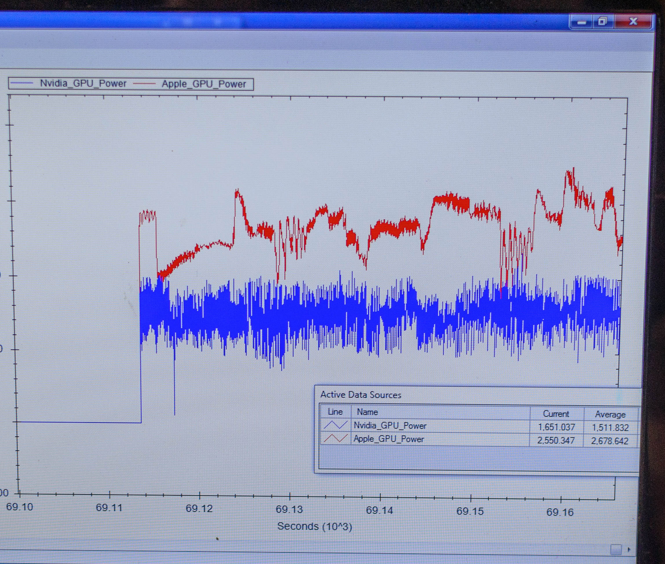

NVIDIA’s tools show the X1’s GPU averages 1.51W over the run of Manhattan. Meanwhile the A8X’s GPU averages 2.67W, over a watt more for otherwise equal performance. This test is especially notable since both SoCs are manufactured on the same TSMC 20nm SoC process, which means that any performance differences between the two devices are solely a function of energy efficiency.
There are a number of other variables we’ll ultimately need to take into account here, including clockspeeds, relative die area of the GPU, and total platform power consumption. But assuming NVIDIA’s numbers hold up in final devices, X1’s GPU is looking very good out of the gate – at least when tuned for power over performance.


194 Comments
View All Comments
esterhasz - Monday, January 5, 2015 - link
Only one of the three devices you mention runs on Denver cores (Nexus 9) and performance reviews have been very uneven for that device, to say the least.PC Perv - Monday, January 5, 2015 - link
Oh I don't know, man. All I know is that every Galaxy tablet has either Exynos or Snapdragon in it.OK, maybe not all of them but I do not think Tegra is in any of them.
kron123456789 - Monday, January 5, 2015 - link
Yeah but it's either Exynos 5420 or Snapdragon 800/801.darkich - Monday, January 5, 2015 - link
Well you dont know much then.Tegra K1 got to market along with the Snapdragon 805 and Exynos 5433.
Out of those three, the K1 took most design wins .
Dont compare the K1 with other Snapdragon and Exynos chips ,and the sea of MTK, Rockchip, Allwinner and Intel atoms chips.
It is an entirely different market
darkich - Monday, January 5, 2015 - link
Clarification- by "most design wins" I was referring to tablet market of courselucam - Wednesday, January 7, 2015 - link
Let's say 2 since one is Nvidia reference tablet and of course it always wins.chizow - Monday, January 5, 2015 - link
@jcwalla, I'm not sure there's "no fruit" from their investment, they are now on their 6th major iteration of Tegra (1-4, K1, X1) with a major variant in Denver K1 and while their marketshare and Tegra revenue won't reflect it, they are clearly the market leader in terms of performance for Android SoCs while going toe-to-toe with the monstrous Apple. Not bad, considering I am positive Apple is probably investing more than Nvidia's yearly revenue in keeping their SoC's relevant. ;)Breaking into an established market and growing a business from scratch is hard, but Nvidia clearly sees this as an important battle that needs to be fought. As a shareholder and tech enthusiast, I agree, in 10 years there's no doubt I would want an Nvidia GPU in whatever handheld/thin device I am using to power my devices.
The problem is that Nvidia lacks the "killer app" that really distinguishes their SoC over others. Even Apple is beginning to understand this as there's nothing on iOS that remotely takes advantage of the A8X's overkill specs. Nvidia needs to grow the Android/mobile gaming market before they really distinguish themselves, and from what I have seen, THAT is their biggest problem right now.
jwcalla - Monday, January 5, 2015 - link
Tegra is an important LOB for NVIDIA, but I'm more talking about how Denver has been received. When it was in the rumor stage, the scuttlebutt seemed to be about how they were going to marry ARMv8 CPU cores with discrete cards and take over the HPC world, etc. Then that got filtered down to "Yeah Denver is just a custom ARMv8 core for Tegra." (Which isn't earth-shattering; Qualcomm and Apple had been doing custom designs for a long time.) And now it doesn't seem like Denver is really anything special at all.But did it not involve a lot of hype, money, and time over all those years?
chizow - Monday, January 5, 2015 - link
Well, I think that HPC embedded ARM core in a massive GPGPU is still a possibility, but again, you're looking a very focused usage scenario, one which I think was pushed back by the process node delays at 20nm and now 16nm FinFET. We have seen since then Nvidia's roadmaps have changed accordingly with some of the features migrating vertically to new generation codenames.But the important point is that Nvidia's investment in mobile makes these options and avenues possible, even if Tegra isn't lightning up the P&L statements every quarter.
Yojimbo - Monday, January 5, 2015 - link
NVIDIA seems to be marrying themselves to IBM in the HPC space, but maybe ARM HPC is a different segment than what PowerPC occupies? I don't know. But IBM has a lot of experience and expertise in the area. Maybe NVIDIA thought they were biting off more than they could chew, maybe the Denver CPU just wasn't performing well enough, or maybe the opportunity with IBM came along because IBM realized they could benefit from NVIDIA as they didn't have anything to compete with Intel's Xeon Phi, and NVIDIA jumped at it.