AMD Radeon HD 7970 Review: 28nm And Graphics Core Next, Together As One
by Ryan Smith on December 22, 2011 12:00 AM EST- Posted in
- GPUs
- AMD
- Radeon
- ATI
- Radeon HD 7000
Building Tahiti & The Southern Islands
Now that we’ve had a chance to go over the basis of the Graphics Core Next architecture, let’s talk about the finished products.
Today AMD will be launching Tahiti, the first GPU of the Southern Islands family. Southern Islands will initially be composed of 3 GPUs: Tahiti, Pitcairn, and Cape Verde. Tahiti is the largest and most powerful member of the Southern Islands family, while Pitcairn and Cape Verde get progressively smaller. AMD has not yet announced the branding or launch dates for Pitcarn and Cape Verde, but it typically takes AMD around 6 months to launch a complete family. As such it’s reasonable to expect that all 3 GPUs will have launched by the end of June although there’s a good likelihood of it happening sooner than that.
All 3 GPUs are based on the GCN architecture, and as family members will have similar features while varying the number of functional units accordingly. Along with the architecture change Southern Islands brings with it a slew of additional features that we’ll get to in the following pages, including Partially Resident Texture (PRT) support, PCIe 3.0, FastHDMI, Direct3D 11.1, and AMD’s fixed-function H.264 encoder, the Video Codec Engine.
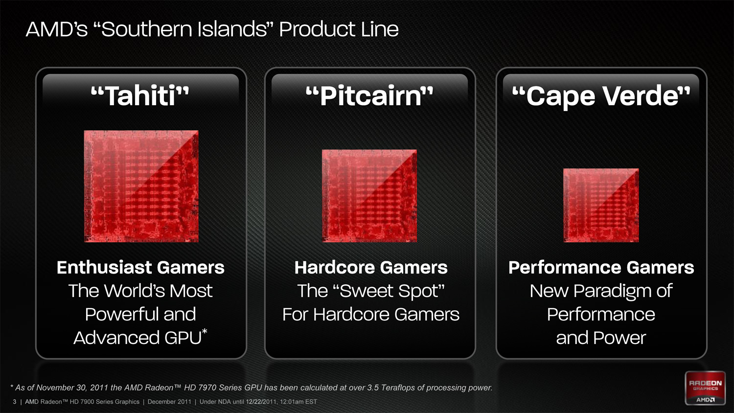
But today is all about Tahiti, so let’s get down to business.
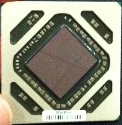
As we quickly covered in our introduction, Tahiti is a 4.31B transistor GPU based on the GCN architecture and built on TSMC’s new 28nm High-K process. Due to TSMC canceling their 32nm process last year AMD has had to wait over 2 years for the next full node rather than taking advantage of the half-node process as they typically do, and as a result the jump from Cayman at 40nm to Tahiti at 28nm is much bigger than with past product launches. Whereas Cayman had 2.64B transistors and a die size of 389mm2, Tahiti has a whopping 63% more transistors than Cayman and yet it’s still smaller, coming in at a slightly more petite 365mm2.
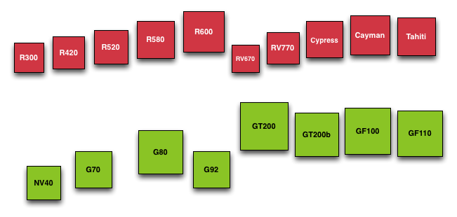
GPU Die Size Comparison
At this point AMD hasn’t provided us with the typical board power values for 7970, but we do know that PowerTune is limited to 250W. In terms of design 7970 is clearly intended to work in similar environments as the 6970, in which case power consumption should be similar to the 6970.
Interestingly enough however we’re hearing that 7970 cards are proving to be very overclockable, which is a good sign for the state of TSMC’s 28nm process, and at the same time a bit distressing. Moore’s Law has continued to hold with respect to transistor density, but the power consumption benefits of using smaller nodes has continued to wane. Having a lot of overclocking headroom means that the 7970 has the potential to be much faster, but it also means that the 7970 (and 28nm GPUs in general) are going to be bottlenecked by power. In which case seeing as how we’re already approaching 300W with single-GPU video cards, the performance gains realized from future fabrication processes would be limited to the ever diminishing returns on power consumption improvements.
Diving deeper into Tahiti, as per the GCN architecture Tahiti’s 2048 SPs are organized into 32 Compute Units. Each of these CUs contains 4 texture units and 4 SIMD units, along with a scalar unit and the appropriate cache and registers. At the 7970’s core clock of 925MHz this puts Tahiti’s theoretical FP32 compute performance at 3.79TFLOPs, while its FP64 performance is ¼ that at 947GFLOPs. As GCN’s FP64 performance can be configured for 1/16, ¼, or ½ its FP32 performance it’s not clear at this time whether the 7970’s ¼ rate was a hardware design decision for Tahiti or a software cap that’s specific to the 7970. However as it’s obvious that Tahiti is destined to end up in a FireStream card we will no doubt find out soon enough.
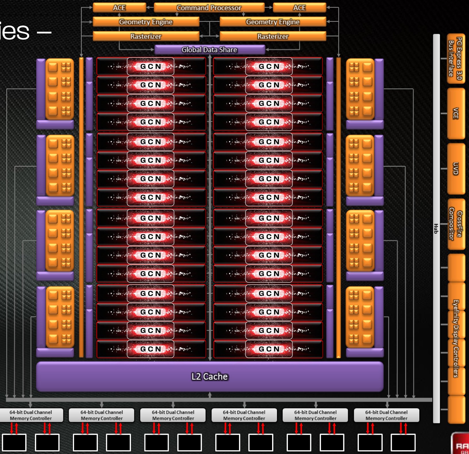
Meanwhile the frontend/command processor for Tahiti is composed of 2 Asynchronous Command Engines (ACEs) and 2 geometry engines. Just as with Cayman each geometry engine can dispatch 1 triangle per clock, giving Tahiti the same theoretical 2 triangle/clock rate as Cayman. As we’ll see however, in practice Tahiti will be much faster than Cayman here due to efficiency improvements.
Looking beyond the frontend and shader cores, we’ve seen a very interesting reorganization of the rest of the GPU as opposed to Cayman. Keeping in mind that AMD’s diagrams are logical diagrams rather than physical diagrams, the fact that the ROPs on Tahiti are not located near the L2 cache and memory controllers in the diagram is not an error. The ROPs have in fact been partially decoupled from the L2 cache and memory controllers, which is also why there are 8 ROP partitions but only 6 memory controllers. Traditionally the ROPs, L2 cache, and memory controllers have all been tightly integrated as ROP operations are extremely bandwidth intensive, making this a very unusual design for AMD to use.
As it turns out, there’s a very good reason that AMD went this route. ROP operations are extremely bandwidth intensive, so much so that even when pairing up ROPs with memory controllers, the ROPs are often still starved of memory bandwidth. With Cayman AMD was not able to reach their peak theoretical ROP throughput even in synthetic tests, never mind in real-world usage. With Tahiti AMD would need to improve their ROP throughput one way or another to keep pace with future games, but because of the low efficiency of their existing ROPs they didn’t need to add any more ROP hardware, they merely needed to improve the efficiency of what they already had.
The solution to that was rather counter-intuitive: decouple the ROPs from the memory controllers. By servicing the ROPs through a crossbar AMD can hold the number of ROPs constant at 32 while increasing the width of the memory bus by 50%. The end result is that the same number of ROPs perform better by having access to the additional bandwidth they need.
The big question right now, and one we don’t have an answer to, is what were the tradeoffs for decoupling the ROPs? Clearly the crossbar design has improved ROP performance through the amount of memory bandwidth they can access, but did it impact anything else? The most obvious tradeoff here would be for potentially higher latency, but there may be other aspects that we haven’t realized yet.
On that note, let’s discuss the memory controllers quickly. Tahiti’s memory controllers aren’t significantly different from Cayman’s but there are more of them, 50% more in fact, forming a 384bit memory bus. AMD has long shied away from non-power of 2 memory busses, and indeed the last time they even had a memory bus bigger than 256bits was with the ill-fated 2900XT, but at this point in time AMD has already nearly reached the practical limits of GDDR5. AMD’s ROPs needed more memory bandwidth, but even more than that AMD needed more memory bandwidth to ensure Tahiti had competitive compute performance, and as such they had little choice but to widen their memory bus to 384bits wide by adding another 2 memory controllers.
It’s worth noting though that the addition of 2 more memory controllers also improves AMD’s cache situation. With 128KB of L2 cache being tied to each memory controller, the additional controllers gave AMD 768KB of L2 cache, rather than the 512KB that a 256bit memory bus would be paired with.


292 Comments
View All Comments
SlyNine - Friday, December 23, 2011 - link
Not really, If Nvidia didn't handicap the CPU version of physx so bad than I'd be fine with it, But Nvidia purposely made the CPU version of phsyx worse totally gimped.CeriseCogburn - Thursday, March 8, 2012 - link
I agree, but that's the way it guy. The amd fans don't care what they and their reviewers pull, and frankly the reviewers would recieve death threats if they didn't comply with amd fanboy demands....So when nvidia had ambient occlusion active for several generations back in a driver add, we were suddenly screamed at that shadows in games suck.... because of course amd didn't have that feature...
That's how the whole thing is set up - amd must be the abused underdog, nvidia must be the evil mis-implementer, until of course amd gets and actual win, or even any win even with 10% IQ performance cheat solidly in place, and any other things like failed AA, poor tessellation performance, no PhysX, etc, etc, etc...
We just must hate nvidia for being better and of course it's all nvidia's fault as they are keeping the poor red radeon down....
If amd radeon has " a perfectly circular algorithm " and it does absolutely nothing and even worse in all games, it is to be praised as an advantage anyway.... and that is still happening to this very day... we ignore shimmer until now, when amd 79xx has a fix for it.... etc..
Dude, that's the way it is man....
Nvidia is the evil, and they're keeping the radeon down...
They throw around money too ( that's unfair as well - and evil ...)
See?
So just pretend anything radeon cannot do that nvidia can doesn't count and is bad, and then make certain nvidia is cut down to radeon level, IQ cheat, no PhysX, AA not turned on, Tesselation turned down, default driver hacks left in place for amd, etc....
Then be sure to cheer when some price perf calc ignoring all the above shows a higher and or lower and card to have a few cents advantage... no free game included, no eyefinity cables... etc.
Just dude... amd = good / nvidia=evil ...
Cool ?
shin0bi272 - Thursday, December 22, 2011 - link
Since I cant edit my comments I have to post this in a second comment instead.According to the released info, Nvidia’s Next Gen flagship GK-100/GK-112 chip which will feature a total f 1024 Shaders (Cuda Cores), 128 texture units (TMUs), 64 ROP’s and a 512-bit GDDR5 Memory interface. The 28nm Next Gen beast would outperform the current Dual chip Geforce GTX590 GPU.
shaboinkin - Thursday, December 22, 2011 - link
Can someone tell me why GPUs tend to have much more transistors than a CPU? I never knew why.Boushh - Thursday, December 22, 2011 - link
Basically it has to do with the difference between programs (= CPU instructions) and graphics (= pixels):A program consists of CPU intructions, many of these instructions depend on output from the previous instruction, Therefore adding more pipelines that can work on the instructions doen't realy work.
A picture consists of pixels, these can be processed in parrallel. So if you double the number of pipelines (= pixels you can work on at the same time), you double the performance.
Therefore CPU's don't have that many transistors. In fact, most transistors in a CPU are in the cache memory not in the actual CPU cores. And GPU's do.
Of course this is hust a simple explenation, the through is much much more complex ;-)
Boushh - Thursday, December 22, 2011 - link
That last line should read:'Of course this is just a simple explanation, the reality is much much more complex'
Reminds me to yet again vote for an EDIT button !!!! Maybe as a christmas present ? PLEASE !!!
shaboinkin - Thursday, December 22, 2011 - link
Interesting...Do you know of a site that goes into the finer details?
Mishera - Wednesday, December 28, 2011 - link
If you're looking for something to specifically answer you question the checking different tech sites. I think realworldtech addressed tis to a degree. Jon Stokes at arstechnica from what I heard wrote some pretty good articles on chip design as well. But if it's a question on chip architecture, reading some textbooks is your best bet. I asked a similar question in the forums before and got some great responses just check my posts.I add to what Boushh said in that for the type of information they process, it's beneficial to have more performance (and not just for graphics). That's why Amd has been pushing to integrate the gpu into the CPU. That's also to a degree show the different philosophy right now between intel and Amd in multicore computing (or the difference between Amd's new gpu architecture vs their previous one).
What it comes down to is optimizing chip design to make use of programs, vice versa. There really is now absolute when dealing with this.
MrSpadge - Thursday, December 22, 2011 - link
It's not like - as stated several times in the article - AMD is wrong about the power target of the HD7970, if they mean the PowerTune limit. Think of it as "the card is built to handle this much heat, and is guaranteed not to exceed it". That doesn't forbid drawing less power. And that's exactly what the HD6970 does: it's got the same "power target", but it uses less of its power budget than the HD7970.Like CPUs, whose real world power consumption is often much less than the TDP.
MrS
Ryan Smith - Thursday, December 22, 2011 - link
PowerTune is a hard cap on power consumption. Given a sufficient workload (i.e. FurMark or OCCT), you can make the card try to consume more power than it is allowed, at which point PowerTune kicks in. Or to put this another way, PowerTune doesn't kick in unless the card is at its limit.PowerTune kicked in for both the 6970 and 7970. In which case both cards should have be limited to 250W.