The NVIDIA GeForce GTX 1080 & GTX 1070 Founders Editions Review: Kicking Off the FinFET Generation
by Ryan Smith on July 20, 2016 8:45 AM ESTFeeding Pascal, Cont: 4th Gen Delta Color Compression
Now that we’ve seen GDDR5X in depth, let’s talk about the other half of the equation when it comes to feeding Pascal: delta color compression.
NVIDIA has utilized delta color compression for a number of years now. However the technology only came into greater prominence in the previous Maxwell 2 generation, when NVIDIA disclosed delta color compression’s existence and offered a basic overview of how it worked. As a reminder, delta color compression is a per-buffer/per-frame compression method that breaks down a frame into tiles, and then looks at the differences between neighboring pixels – their deltas. By utilizing a large pattern library, NVIDIA is able to try different patterns to describe these deltas in as few pixels as possible, ultimately conserving bandwidth throughout the GPU, not only reducing DRAM bandwidth needs, but also L2 bandwidth needs and texture unit bandwidth needs (in the case of reading back a compressed render target).
Since its inception NVIDIA has continued to tweak and push the technology for greater compression and to catch patterns they missed on prior generations, and Pascal in that respect is no different. With Pascal we get the 4th generation of the technology, and while there’s nothing radical here compared to the 3rd generation, it’s another element of Pascal where there has been an iterative improvement on the technology.
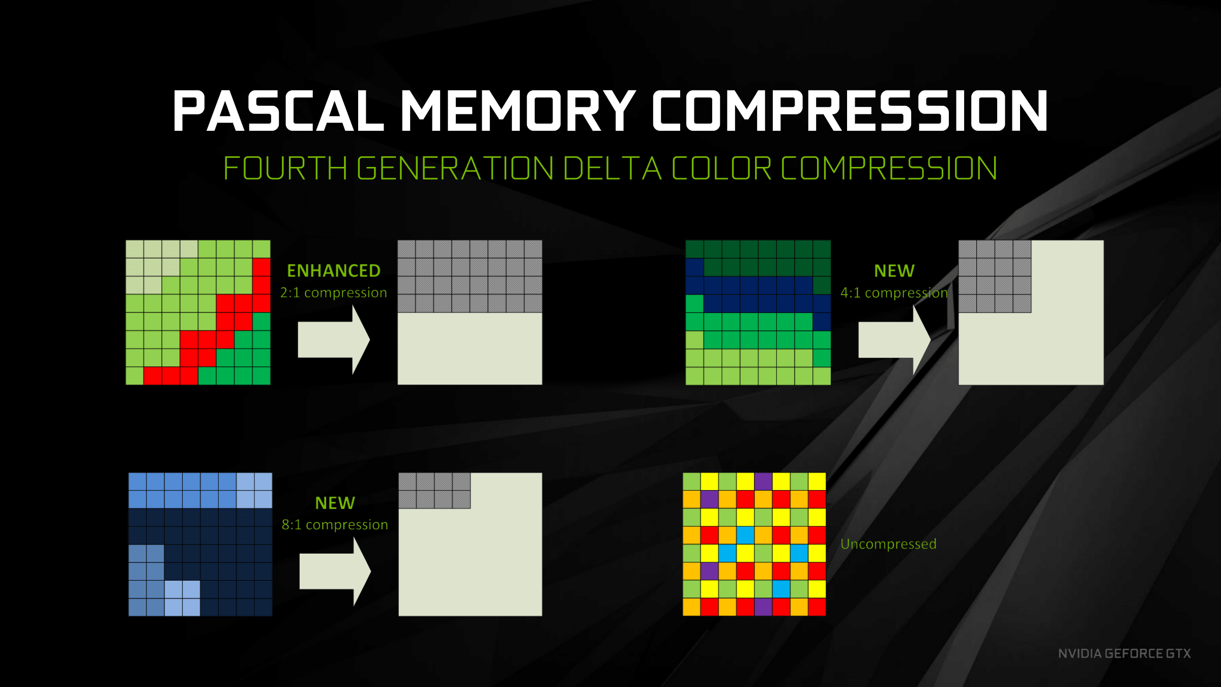
New to Pascal is a mix of improved compression modes and new compression modes. 2:1 compression mode, the only delta compression mode available up through the 3rd generation, has been enhanced with the addition of more patterns to cover more scenarios, meaning NVIDIA is able to 2:1 compress blocks more often.
Meanwhile, new to delta color compression with Pascal is 4:1 and 8:1 compression modes, joining the aforementioned 2:1 mode. Unlike 2:1 mode, the higher compression modes are a little less straightforward, as there’s a bit more involved than simply the pattern of the pixels. 4:1 compression is in essence a special case of 2:1 compression, where NVIDIA can achieve better compression when the deltas between pixels are very small, allowing those differences to be described in fewer bits. 8:1 is more radical still; rather an operating on individual pixels, it operates on multiple 2x2 blocks. Specifically, after NVIDIA’s constant color compressor does its job – finding 2x2 blocks of identical pixels and compressing them to a single sample – the 8:1 delta mode then applies 2:1 delta compression to the already compressed blocks, achieving the titular 8:1 effective compression ratio.
Overall, delta color compression represents one of the interesting tradeoffs NVIDIA has to make in the GPU design process. The number of patterns is essentially a function of die space, so NVIDIA could always add more patterns, but would the memory bandwidth improvements be worth the real cost of die space and the power cost of those transistors? Especially since NVIDIA has already implemented the especially common patterns, which means new patterns likely won’t occur as frequently. NVIDIA of course pushed ahead here, thanks in part to the die and power savings of 16nm FinFET, but it gives us an idea of where they might (or might not) go in future generations in order to balance the costs and benefits of the technology, with less of an emphasis on patterns and instead making more novel use of those patterns.
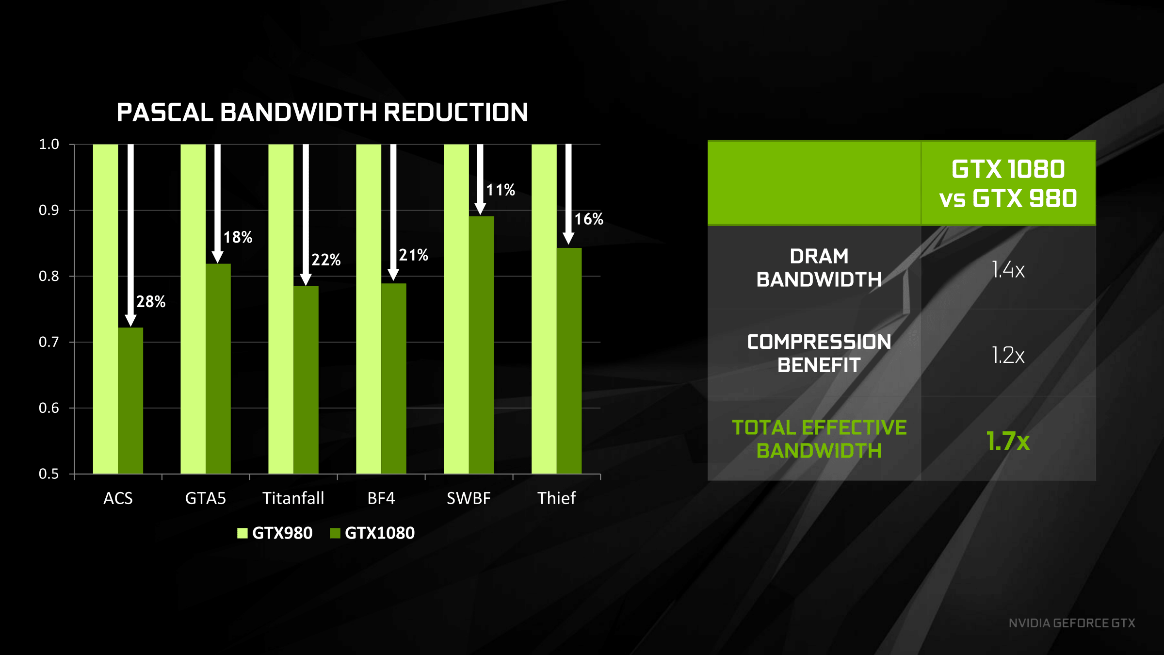
To put all of this in numbers, NVIDIA pegs the effective increase in memory bandwidth from delta color compression alone at 20%. The difference is of course per-game, as the effectiveness of the tech depends on how well a game sticks to patterns (and if you ever create a game with random noise, you may drive an engineer or two insane), but 20% is a baseline number for the average. Meanwhile for anyone keeping track of the numbers over Maxwell 2, this is a bit less than the gains with NVIDIA’s last generation architecture, where the company claimed the average gain was 25%.
The net impact then, as NVIDIA likes to promote it, is a 70% increase in the total effective memory bandwidth. This comes from the earlier 40% (technically 42.9%) actual memory bandwidth gains in the move from 7Gbps GDDR5 to 10Gbps GDDR5X, coupled with the 20% effective memory bandwidth increase from delta compression. Keep those values in mind, as we’re going to get back to them in a little bit.
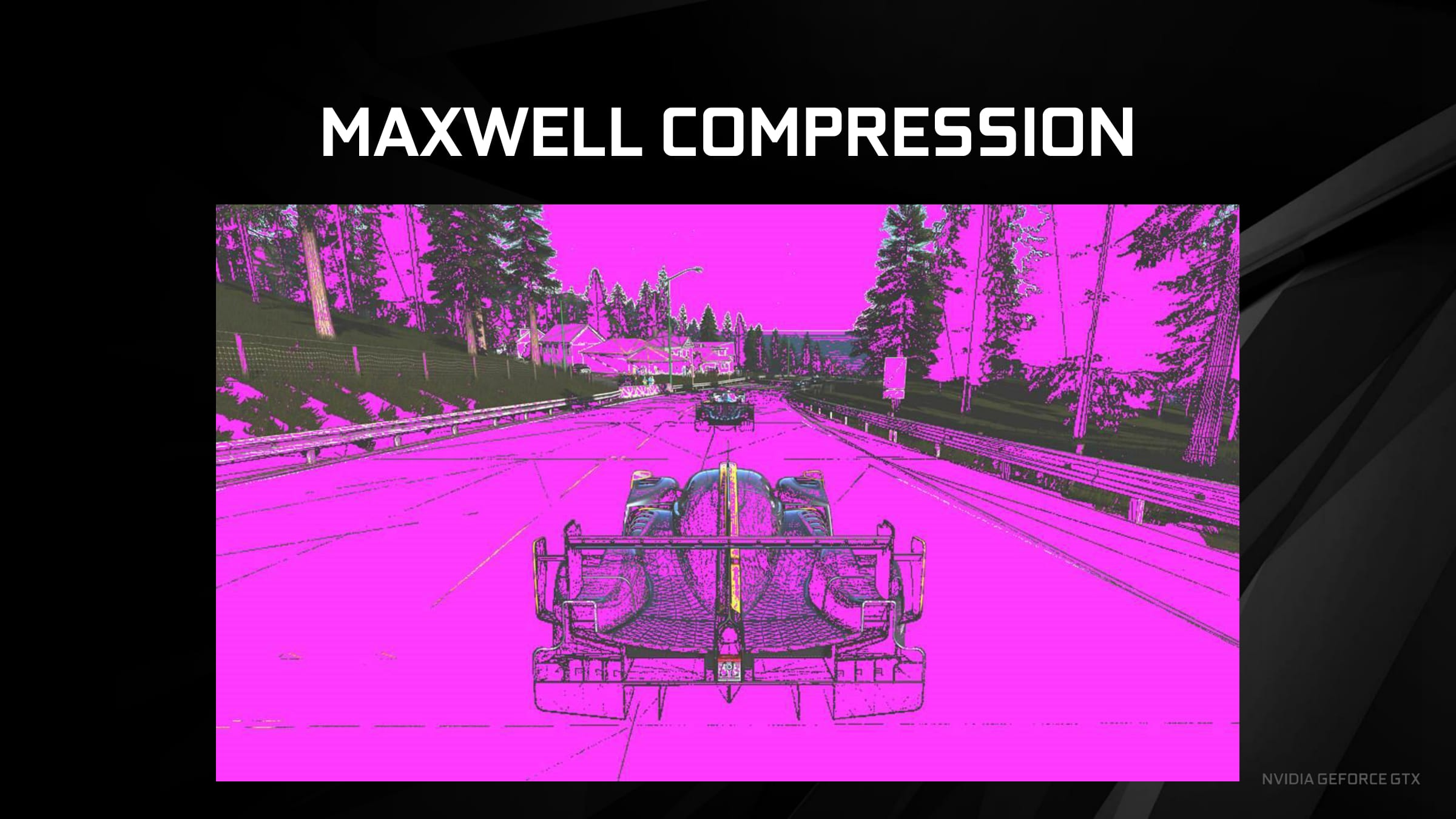
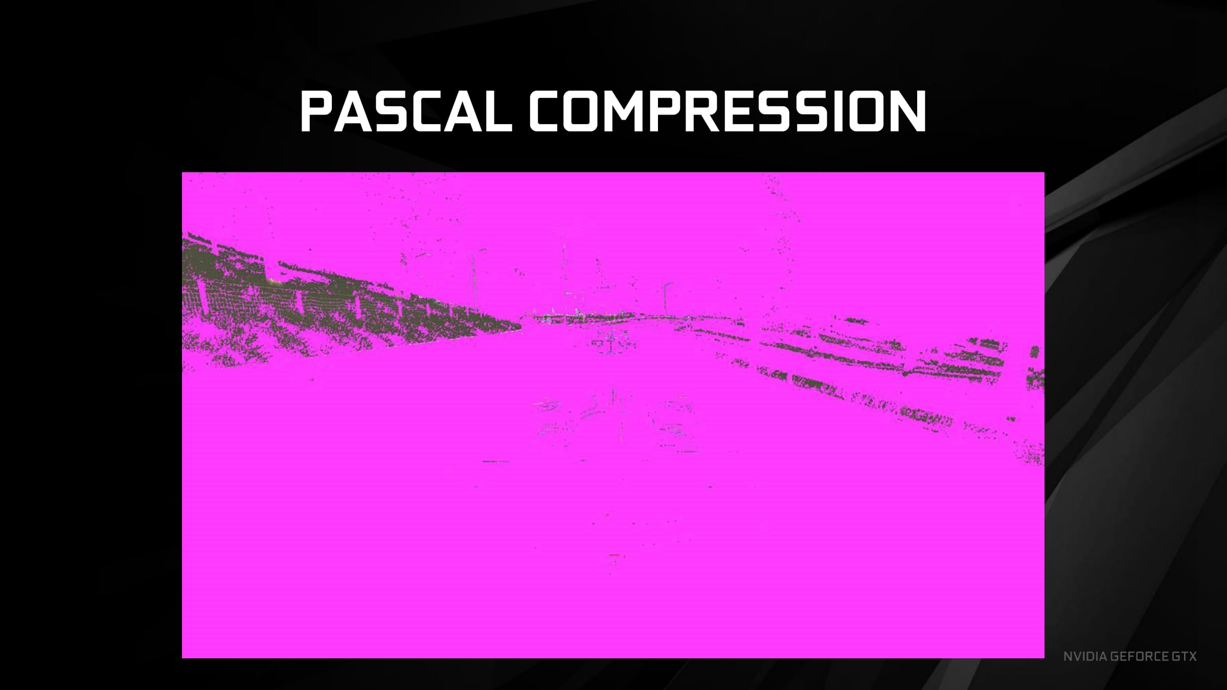
Meanwhile from a graphical perspective, to showcase the impact of delta color compression, NVIDIA sent over a pair of screenshots for Project Cars, colored to show what pixels had been compressed. Shown in pink, even Maxwell can compress most of the frame, really only struggling with finer details such as the trees, the grass, and edges of buildings. Pascal, by comparison, gets most of this. Trees and buildings are all but eliminated as visually distinct uncompressed items, leaving only patches of grass and indistinct fringe elements. It should be noted that these screenshots have most likely been picked because they’re especially impressive – seeing as how not all games compress this well – but it’s none the less a potent example of how much of a frame Pascal can compress.
Finally, while we’re on the subject of compress, I want to talk a bit about memory bandwidth relative to other aspects of the GPU. While Pascal (in the form of GTX 1080) offers 43% more raw memory bandwidth than GTX 980 thanks to GDDR5X, it’s important to note just how quickly this memory bandwidth is consumed. Thanks to GTX 1080’s high clockspeeds, the raw throughput of the ROPs is coincidentally also 43% higher. Or we have the case of the CUDA cores, whose total throughput is 78% higher, shooting well past the raw memory bandwidth gains.
While it’s not a precise metric, the amount of bandwidth available per FLOP has continued to drop over the years with NVIDIA’s video cards. GTX 580 offered just short of 1 bit of memory bandwidth per FLOP, and by GTX 980 this was down to 0.36 bits/FLOP. GTX 1080 is lower still, now down to 0.29bits/FLOP thanks to the increase in both CUDA core count and frequency as afforded by the 16nm process.
| NVIDIA Memory Bandwidth per FLOP (In Bits) | ||||||
| GPU | Bandwidth/FLOP | Total FLOPs | Total Bandwidth | |||
| GTX 1080 | 0.29 bits | 8.87 TFLOPs | 320GB/sec | |||
| GTX 980 | 0.36 bits | 4.98 TFLOPs | 224GB/sec | |||
| GTX 680 | 0.47 bits | 3.25 TFLOPs | 192GB/sec | |||
| GTX 580 | 0.97 bits | 1.58 TFLOPs | 192GB/sec | |||
The good news here is that at least for graphical tasks, the CUDA cores generally aren’t the biggest consumer of DRAM bandwidth. That would fall to the ROPs, which are packed alongside the L2 cache and memory controllers for this very reason. In that case GTX 1080’s bandwidth gains keep up with the ROP performance increase, but only by just enough.
The overall memory bandwidth needs of GP104 still outpace the memory bandwidth gains from GDDR5X, and this is why features such as delta color compression are so important to GP104’s performance. GP104 is perpetually memory bandwidth starved – adding more memory bandwidth will improve performance, as we’ll see in our overclocking results – and that means that NVIDIA will continue to try to conserve memory bandwidth usage as much as possible through compression and other means. How long they can fight this battle remains to be seen – they already encounter diminishing returns in some cases – but in the meantime this allows NVIDIA to utilize smaller memory buses, keeping down the die size and power costs of their GPUs, making PCB costs cheaper, and of course boosting profit margins at the same time.


200 Comments
View All Comments
Ryan Smith - Friday, July 22, 2016 - link
2) I suspect the v-sync comparison is a 3 deep buffer at a very high framerate.lagittaja - Sunday, July 24, 2016 - link
1) It is a big part of it. Remember how bad 20nm was?The leakage was really high so Nvidia/AMD decided to skip it. FinFET's helped reduce the leakage for the "14/16"nm node.
That's apples to oranges. CPU's are already 3-4Ghz out of the box.
RX480 isn't showing it because the 14nm LPP node is a lemon for GPU's.
You know what's the optimal frequency for Polaris 10? 1Ghz. After that the required voltage shoots up.
You know, LPP where the LP stands for Low Power. Great for SoC's but GPU's? Not so much.
"But the SoC's clock higher than 2Ghz blabla". Yeah, well a) that's the CPU and b) it's freaking tiny.
How are we getting 2Ghz+ frequencies with Pascal which so closely resembles Maxwell?
Because of the smaller manufacturing node. How's that possible? It's because of FinFET's which reduced the leakage of the 20nm node.
Why couldn't we have higher clockspeeds without FinFET's at 28nm? Because power.
28nm GPU's capped around the 1.2-1.4Ghz mark.
20nm was no go, too high leakage current.
16nm gives you FinFET's which reduced the leakage current dramatically.
What does that enable you to do? Increase the clockspeed..
Here's a good article
http://www.anandtech.com/show/8223/an-introduction...
lagittaja - Sunday, July 24, 2016 - link
As an addition to the RX 480 / Polaris 10 clockspeedGCN2-GCN4 VDD vs Fmax at avg ASIC
http://i.imgur.com/Hdgkv0F.png
timchen - Thursday, July 21, 2016 - link
Another question is about boost 3.0: given that we see 150-200 Mhz gpu offset very common across boards, wouldn't it be beneficial to undervolt (i.e. disallow the highest voltage bins corresponding to this extra 150-200 Mhz) and offset at the same time to maintain performance at lower power consumption? Why did Nvidia not do this in the first place? (This is coming from reading Tom's saying that 1060 can be a 60w card having 80% of its performance...)AnnonymousCoward - Thursday, July 21, 2016 - link
NVIDIA, get with the program and support VESA Adaptive-Sync already!!! When your $700 card can't support the VESA standard that's in my monitor, and as a result I have to live with more lag and lower framerate, something is seriously wrong. And why wouldn't you want to make your product more flexible?? I'm looking squarely at you, Tom Petersen. Don't get hung up on your G-sync patent and support VESA!AnnonymousCoward - Thursday, July 21, 2016 - link
If the stock cards reach the 83C throttle point, I don't see what benefit an OC gives (won't you just reach that sooner?). It seems like raising the TDP or under-voltaging would boost continuous performance. Your thoughts?modeless - Friday, July 22, 2016 - link
Thanks for the in depth FP16 section! I've been looking forward to the full review. I have to say this is puzzling. Why put it on there at all? Emulation would be faster. But anyway, NVIDIA announced a new Titan X just now! Does this one have FP16 for $1200? Instant buy for me if so.Ryan Smith - Friday, July 22, 2016 - link
Emulation would be faster, but it would not be the same as running it on a real FP16x2 unit. It's the same purpose as FP64 units: for binary compatibility so that developers can write and debug Tesla applications on their GeForce GPU.hoohoo - Friday, July 22, 2016 - link
Excellent article, Ryan, thank you!Especially the info on preemption and async/scheduling.
I expected the preemption mght be expensive in some circumstances, but I didn't quite expect it to push the L2 cache though! Still this is a marked improvement for nVidia.
hoohoo - Friday, July 22, 2016 - link
It seems like the preemption is implemented in the driver though? Are there actual h/w instructions to as it were "swap stack pointer", "push LDT", "swap instruction pointer"?