Analyzing Falkor’s Microarchitecture: A Deep Dive into Qualcomm’s Centriq 2400 for Windows Server and Linux
by Ian Cutress on August 20, 2017 11:00 AM EST- Posted in
- CPUs
- Qualcomm
- Enterprise
- SoCs
- Enterprise CPUs
- ARMv8
- Centriq
- Centriq 2400
Getting Intimate with Falkor: The Back End
The meat and potatoes of Getting Things Done™ is in the core logic – processing instructions with the right data to get the output. The Falkor design has eight of these execution ports: two for load/data, three for ALU/INT, two for FP/vector extensions, and one for direct branches.
The Back End: Load/Store and the L1-Data Cache
The load and store units are usually some of the most vital elements to the design, and here Qualcomm implements 1x128-bit Load and 1x128-bit Store per cycle. Unlike some other competitor designs, there is one unit specifically for load and one specifically for store, rather than issuing two of the same per cycle. These two units have a 3-cycle latency to a hit in the L1-Data cache, which is one cycle faster than most of the competition.
In order to get the latency low, the L1-D cache has to be designed appropriately. So here is a 32KB 8-way design, supporting 64-byte lines but also implementing a write-through strategy. This means that any data committed to L1-D will also be written to the L2. Hardened veterans may recall that the write-through policy was a sizeable bottleneck on AMD’s early Bulldozer designs, so the hope here is that Qualcomm won’t fall into the same trap. The L1-D also supports read-allocate and write-no-allocate modes with split virtual and physical tag addressing.
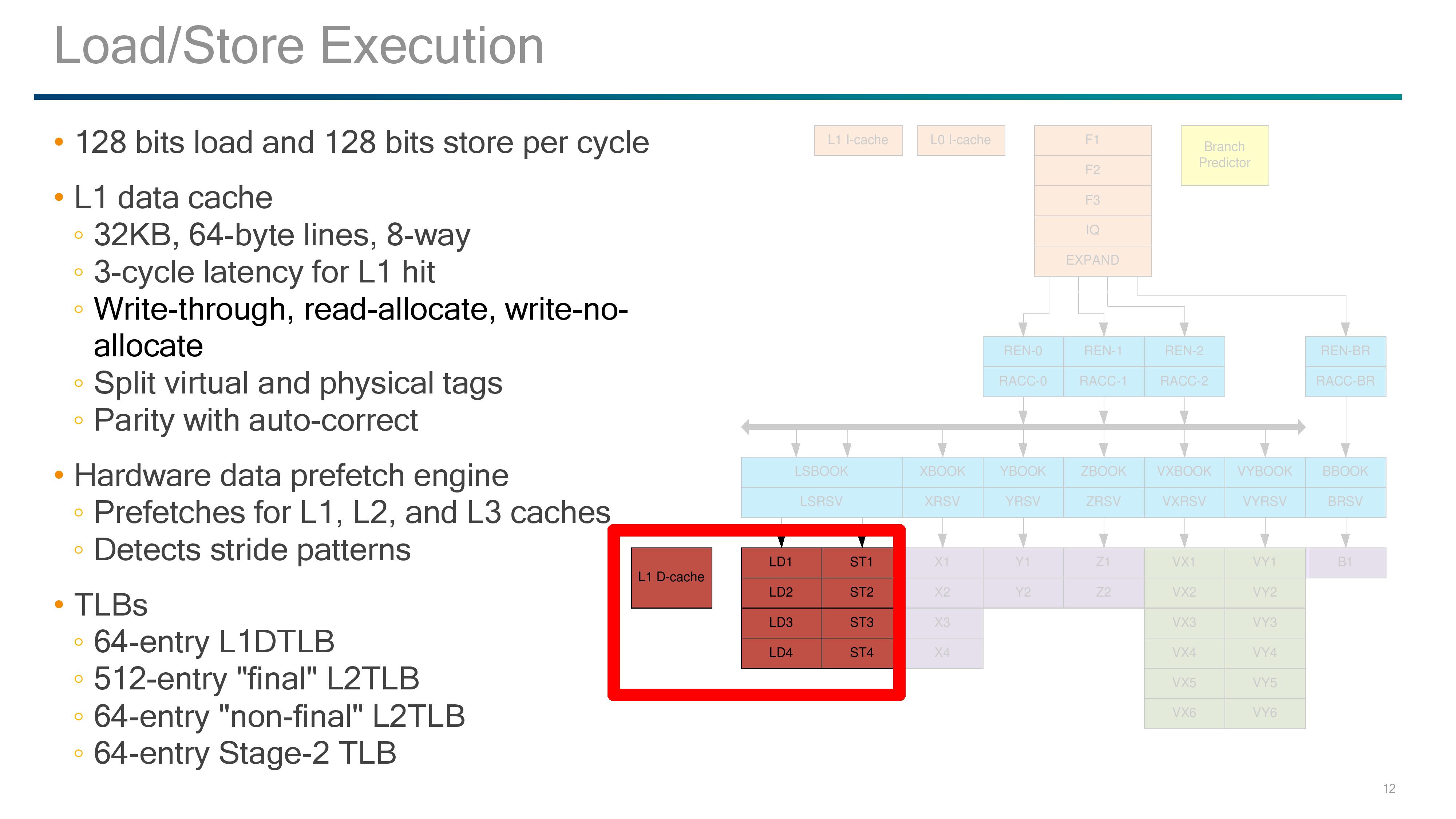
If a miss occurs on the L1-data cache, hardware data prefetchers are used to probe the L2 and L3 caches. Mechanisms are in place to also detect stride pattern access and compensate accordingly. There are two levels of data TLB in place, although as written it comes across as a four-level TLB. It starts with a 64-entry level 1 DTLB, then a larger 512-entry level 2 ‘final’ DTLB. This is backed by a 64-entry level 2 ‘non-final’ DTLB and another 64-entry ‘stage 2’ TLB.
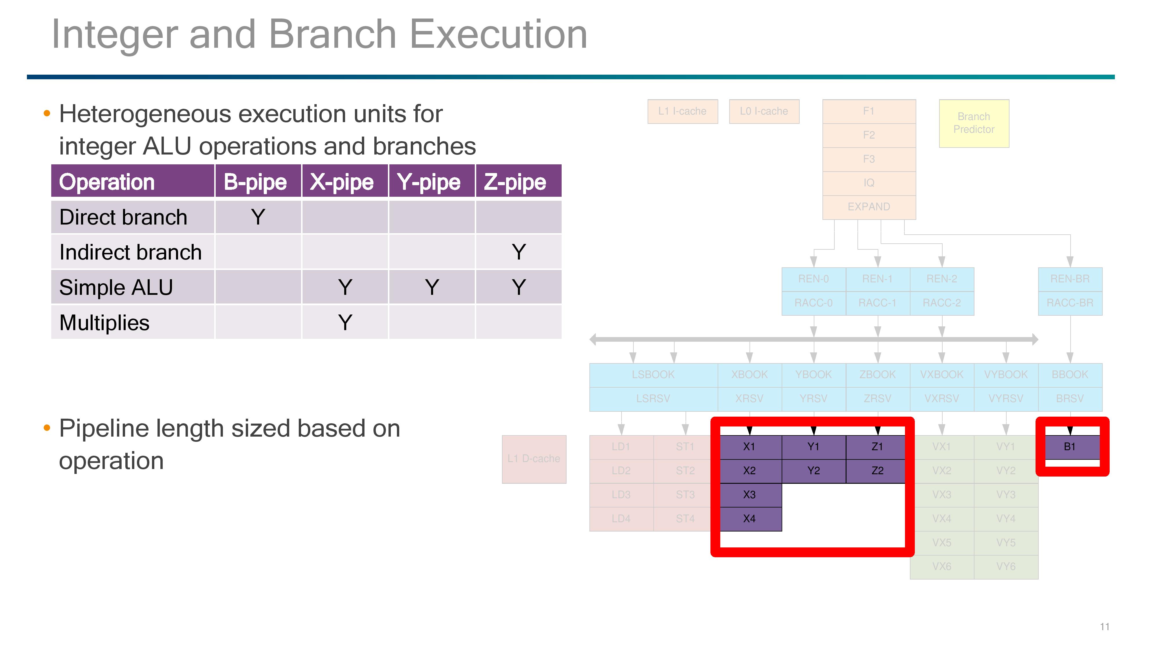
The Back End: ALUs, Vector Extensions, and Branches
On the simple ALU side of the execution ports, Qualcomm labels theses as B, X, Y, and Z-pipes, with a mixed functionality between them and they have different pipeline lengths based on which pipe is needed.
B is for the Branch Pipe, which is for direct branches through the branch side of the decode/rename/queue of the back-end.
The XYZ pipes all perform simple ALU tasks, however only the X pipe can perform MUL operations and takes four stages, and the Z-pipe is the only one for indirect branches. The Y is a simpler ALU-only pipe, with the Y and Z pipe both taking two stages.
The pipes that Qualcomm did not talk about are the VX and VY pipes, which both come in at six stages each. V in this case likely stands for vectors, and may represent traditional NEON/FP operations found in the smartphone cores in mobile or perhaps the new Vector Extensions (VX?) which ARM introduced last year but have so far not been announced in any commercial product. Vector Extensions would allow for 128-2048 bit wide FP compute, and the idea is that the code required for implementing the vector extensions should be agnostic to how big the vector units actually are. Under ARM’s description, the pipeline should be able to process the data appropriately (although this has a knock on effects for latency if not configured for the ideal vector width).


41 Comments
View All Comments
tipoo - Sunday, August 20, 2017 - link
Big ARM server CPUs will be interesting. The ISA is very sane and scalable, if the investment and demand was there it would have no issue getting to where large x86 cores are, the ISA was never the limit.Then we can see if they can actually exceed them.
Kevin G - Sunday, August 20, 2017 - link
This makes me wish that Apple would license their cores to 3rd parties. Recent Apple cores are getting very close to where x86 lies per clock and they've certainly exceeded x86 in performance/watt in the ultra mobile space (granted Intel's last round of ultra mobile chips was flat out cancelled, skewing such a comparison).Considering Apple's work in ultra mobile, I find it believable that a higher performance per clock design in the server space is feasible for an ARM design. A company with enough resources just needs to do it.
iwod - Sunday, August 20, 2017 - link
If the leaked numbers for A11 were true then Apple may have exceeded the performance / clock against Intel x86 as well.While Apple are highly unlikely to ever license their Cores out, I wish they could use those Cores and make an Xserve Server Come back.
peevee - Monday, August 21, 2017 - link
XServe died because of their own OS. Nobody is interested in anything but Linux (and sometimes a little Windows).But they could have sold it with Linux though.
Dr. Swag - Sunday, August 20, 2017 - link
Apple never will though, since it's Apple we're talking about. They keep their tech to themselves to give themselves the advantage.name99 - Sunday, August 20, 2017 - link
The only benchmarks that exist are geekbench4 and the browser benchmarks against Apple laptop hardware. By THOSE benchmarks A9X matched Intel in IPC and A10X exceeds by around 15%.This is clearly an area that draws out the crazies in full screaming mode because a lot of assumptions have to be made (for example the most realistic assumption is that the high-end Intel scores occur at the maximum turbo frequency, but the crazies will insist that, no, you have to normalize to the baseline intel frequency for that particular CPU). Or you get the insistence that the ONLY measurement that matters is against SPEC2006 compiled with icc, which runs into the issues that icc has MASSIVE effects on SPEC; and that no SPEC numbers in any form exist for the A10/A10X.
At the end of the day, it boils down to "what is your goal?" If your goal is an honest comparison of the two processor families, the best data available suggests the summary I gave. If your goal is "my CPU can beat up your CPU" then all the data in the world presumably won't change your mind, and the best data of all is non-existent data (like the certain claims as to how the A10X would or would not behave on SPEC2006).
Final point. It is not at all implausible, IMHO, that Apple have a plan, and have already started proceeding down it, for ARM in their data centers. After all, why not? It saves them money, it allows them to run at their pace not Intel's (eg install AI or compression or encryption accelerators as they need them) and provides better security (both security through obscurity and not having as large an attack surface as Intel).
But why would they talk about it? Apple says nothing ever, unless they have to. No way they would advertise to their competitors the extent to which they have comparative advantage through use of their own data warehouse chips (for at least some purposes).
zodiacfml - Monday, August 21, 2017 - link
Not sa fast. Apple's SoC's are huge in die size which is the reason for their performance. They are as big or bigger than Intel Core. The best part for comparison are the Core M parts. There is little or no business for Apple to do this. There are rumors using Apple SoC on a Macbook Air but that will make little sense as they will to need port OSX to ARM. Again, that is not a good idea as Macbook Pro nor the Mac Pros will continue with OSX .cdillon - Monday, August 21, 2017 - link
Apple has already ported OSX to ARM, and they call it "iOS". It's not going to be as big a deal as you think to get OSX as we know it to run in ARM. Not only that, but they already have experience with juggling two processor architectures (PPC and x86) at the same time in one OS.extide - Monday, August 21, 2017 - link
And 68k to PPC, back in the dayname99 - Monday, August 21, 2017 - link
Apple's SoCs are not huge, neither are their cores.The iPhone SoC's tend to hover around 100 to 120mm^2, the iPad SoCs sometime reach 150, though the A10X is below 100.
The cores are a few mm^2. Eyeballing it, I'd say the entire CPU complex (2 large cores, two small cores, and L2) is about 12mm^2. This is substantially larger than ARM cores (four A73s+their L2 in the same process technology would fit in 8mm^2) but substantially smaller than Intel (an Intel core these days runs at around 8mm^2 in Intels 14nm).