Analyzing Falkor’s Microarchitecture: A Deep Dive into Qualcomm’s Centriq 2400 for Windows Server and Linux
by Ian Cutress on August 20, 2017 11:00 AM EST- Posted in
- CPUs
- Qualcomm
- Enterprise
- SoCs
- Enterprise CPUs
- ARMv8
- Centriq
- Centriq 2400
Getting Intimate with Falkor: The Front End
So we have to admit that we were surprised by Qualcomm releasing so much information about the pipeline. When we’ve ever asked the mobile CPU team about Krait and Kryo, we usually hit a brick wall, left with a PR answer of a ‘custom core design’ or the guide of ‘protecting our design’. So when Falkor was offered on a plate, we grabbed a knife and a chopstick to devour the soup at hand.
The headline features are as follows:
- Variable length pipelines, 10-15 stage depending on instruction
- 4-wide decode (3 + 1 branch)
- 8-wide out-of-order dispatch
- 8 execution ports
- Micro-op cache / L0 I-cache with Way prediction
- Retire 4/cycle usually (some situations >4)
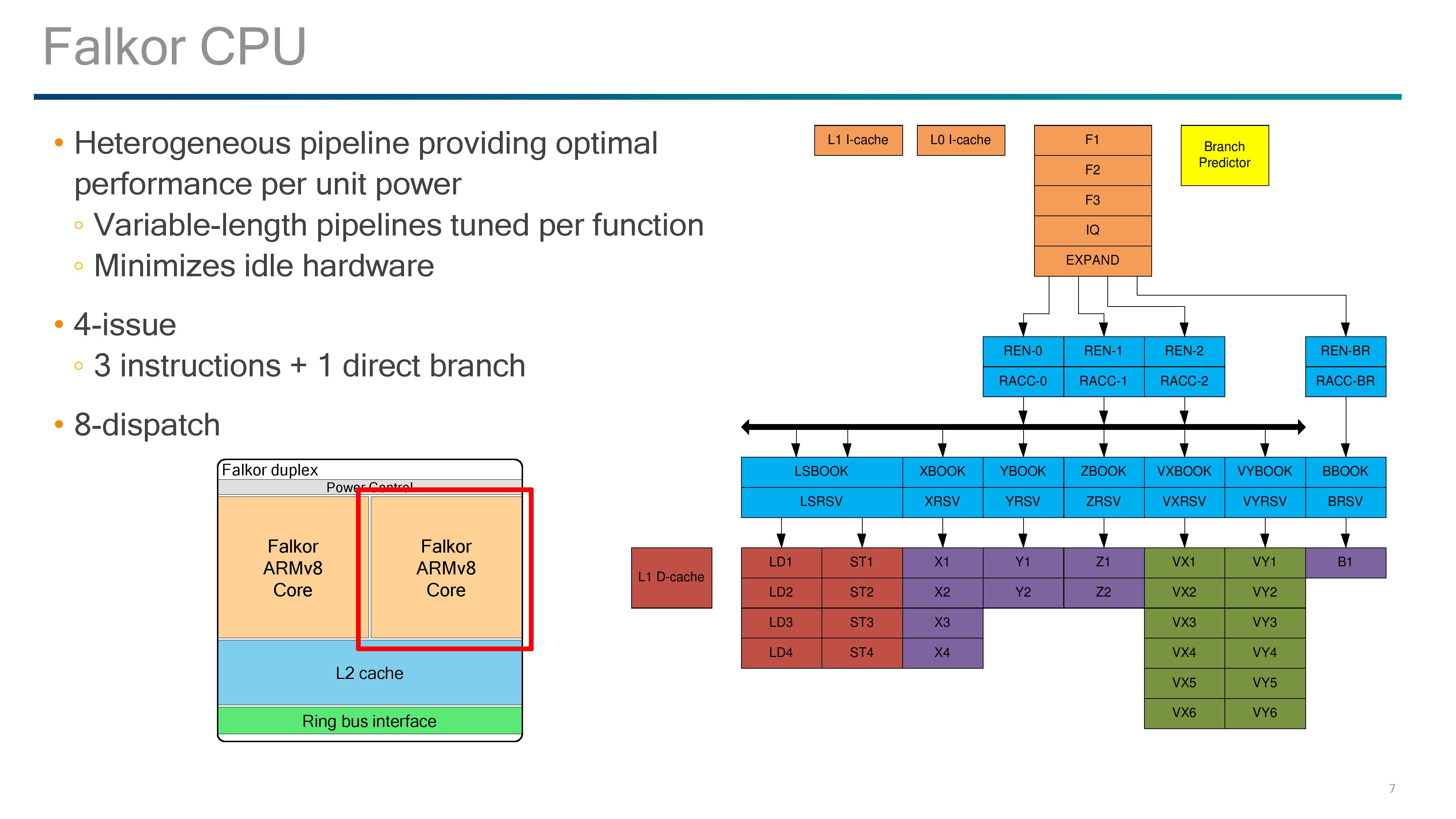
Much like most modern cores and those built on ARM’s instruction sets, pipeline lengths vary for the different execution ports, and Qualcomm states that these are tuned depending on the instruction at play.
Just to add some terminology changes in here: what Intel calls a scheduler, ARM calls an Issue Queue, and Qualcomm calls a ‘Reserve’.
We start with a 4-stage instruction fetch, with the design able to fetch up to four instructions per cycle. These go into a single stage decode that converts the instructions into micro-ops, with most instructions becoming a single micro-op. Branches out of the decode are fed into their own branch rename stage and issue queue, before hitting its own execution port. Micro-ops not fed into the branch stage go into the single-stage rename and single-stage ‘register acccess’ followed by the out-of-order dispatch window.
Up to eight instructions can move into the two-stage Reserves/issue queues, with each execution port having one Reserve except for the load/store units which have a combined Reserve. Loads and stores take 4 stages, ALUs take 2 stages (most) or 4 stages (MUL), while FP and vector pipes take six stages.
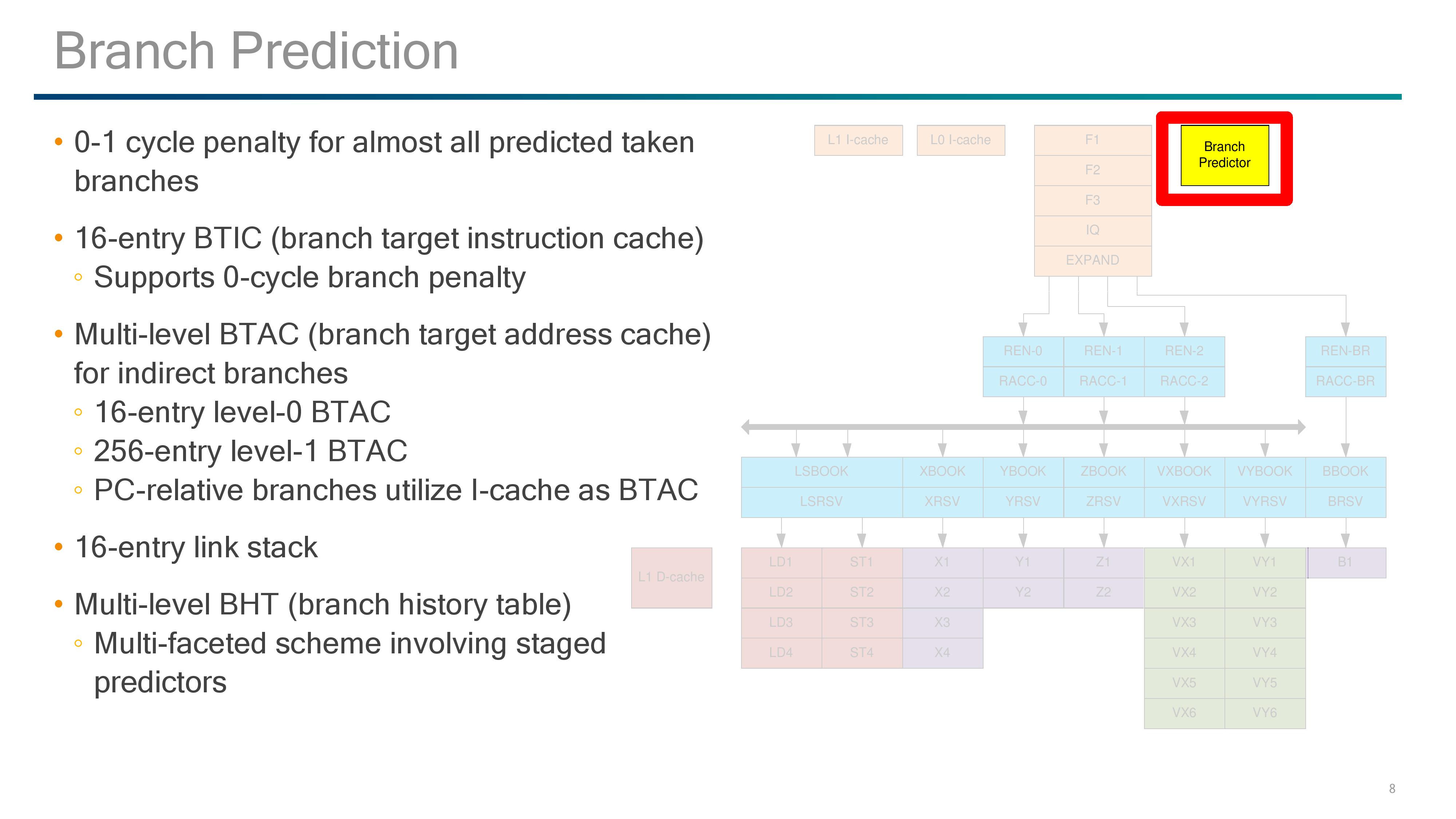
For the fetch stages of the pipeline, Qualcomm doesn’t say much about its prefetch policies here. However we do have information about the branch predictor and L0/L1 caches.
The Front End: Prefetch and Branch Predictor
Qualcomm has implemented a custom branch predictor, and the design gives a 0-1 cycle latency penalty for taking most predicted branches. For instructions, there is a 16-entry branch target instruction cache (BTIC) that supports 0-cycle access, and for addresses there is a two-level branch target address cache (BTAC) for indirect branches: a 16-entry level 0 and a 256-entry level 1. This combines with the 16-entry link stack and multi-level branch history table for predictions.
The Front End: L0/L1 Instruction Caches
The instruction caches are an interesting part of the design, with Qualcomm implementing an L0 I-cache and an L1 I-cache. Qualcomm has implemented L0 caches before, since Krait, but when I initially saw it in this design I instantly thought it looks like a micro-op cache. (in LLVM commits it even states it as a micro-op cache). Normally the test is that if it walks like a micro-op cache and talks like a micro-op cache then it’s a micro-op cache, but the difference here is that rather than storing already-decoded micro-ops, it stores instructions ready to decode.
The special element to the L0 instruction cache here is that it is Way-predicted, meaning that the cache is checked for the instruction as the prefetch also checks the L1. As the L0 is smaller and closer to the event, it offers a 0-cycle latency for any instruction that achieves an L1 hit. The L0 sits at 24 KB, using 64-byte lines and 3-way associativity, but due to the way prediction, the L0 itself is transparent to software and will be seen as part of the L1 cache when metrics probe the size and capability.
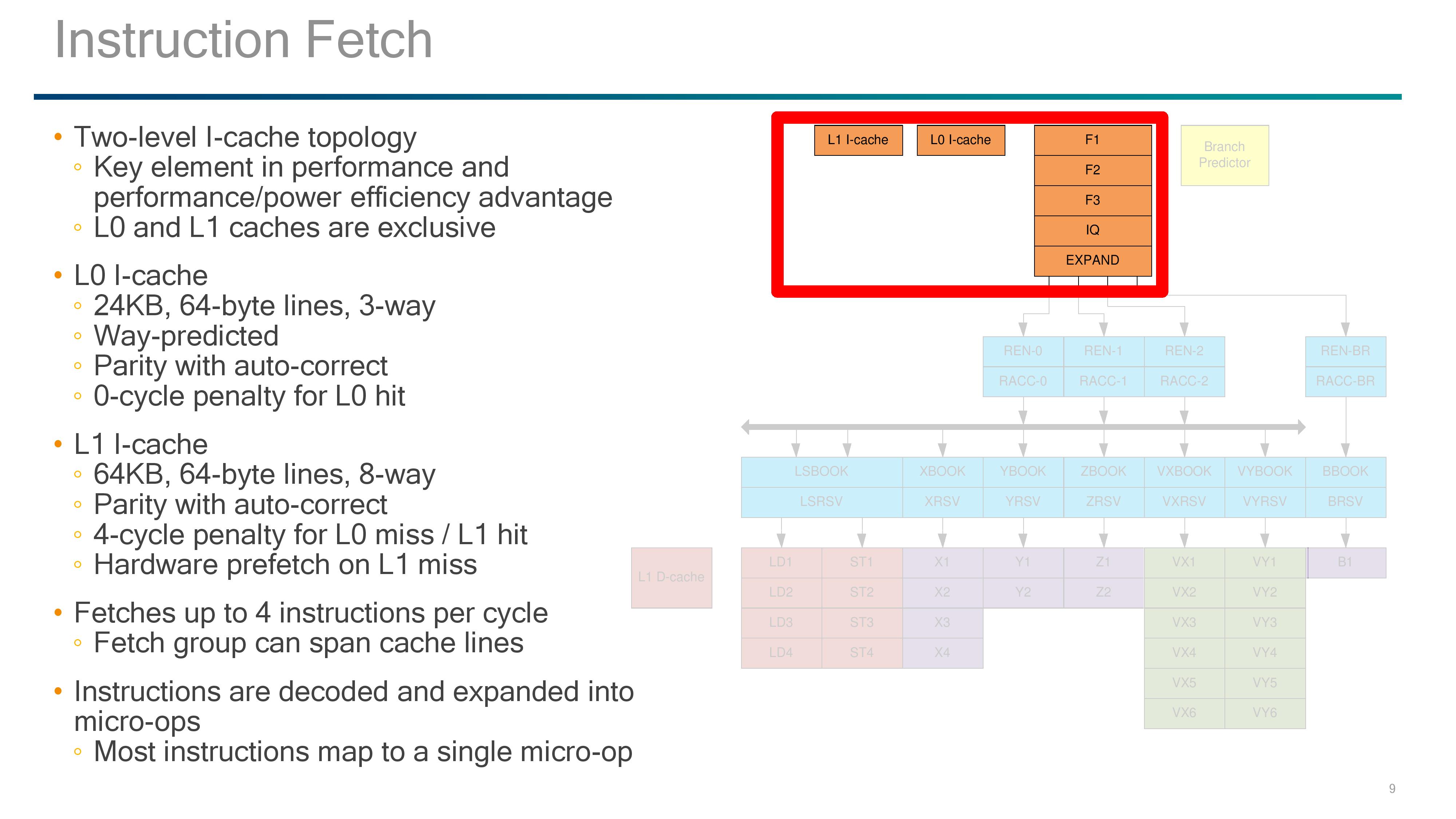
The L1 I-cache is 64KB, which is similar to other ARM architecture core designs, and also uses 64-byte lines but with an 8-way associativity. To software, as the L0 is transparent, the L1 I-cache will show as an 88KB cache. Both the L0 and L1 have parity with auto-correct, and the L1-I has a four cycle penalty on an L0 miss. An L1 miss will initiate a hardware prefetch.
Instructions that go through the fetch end up in the decoders, with the Falkor design supporting 4-issue decode (3 decode + one branch).
The Front End: Rename, Register Access and Reserve (Rename and Dispatch)
It’s worth noting at this point that Qualcomm’s slides seem to make instructions and micro-ops interchangeable at this point, or rather use the term ‘instruction’ where they mean ‘micro-op’.
Direct branches out of the decoder hit their own rename and dispatch pipeline and execution, so the main focus is on the three other decoded micro-ops. Each of these hits the rename and completion buffer, which can support up to 256-entries.
The Qualcomm diagram gets a bit odd here as after the rename/register access stages, the micro-ops hit the out-of-order dispatch buffer. This supports 76 committed micro-ops ready for dispatch or retirement while 128 uncommitted micro-ops can remain in flight, although Qualcomm doesn’t state if these numbers include the Direct Branch decode (it’s worth noting that A73/A75 do not, but A53 does).
The dispatch buffer can push through eight micro-ops per cycle into the reserve stations/issue queues, although only one reserve will serve each execution port, much like a Cortex-A75 design. This means that in order to dispatch eight per cycle, it needs one of each of the execution ports in play. The exceptions to the rule are the two load/store units that use a combined reserve station.


41 Comments
View All Comments
tipoo - Sunday, August 20, 2017 - link
Big ARM server CPUs will be interesting. The ISA is very sane and scalable, if the investment and demand was there it would have no issue getting to where large x86 cores are, the ISA was never the limit.Then we can see if they can actually exceed them.
Kevin G - Sunday, August 20, 2017 - link
This makes me wish that Apple would license their cores to 3rd parties. Recent Apple cores are getting very close to where x86 lies per clock and they've certainly exceeded x86 in performance/watt in the ultra mobile space (granted Intel's last round of ultra mobile chips was flat out cancelled, skewing such a comparison).Considering Apple's work in ultra mobile, I find it believable that a higher performance per clock design in the server space is feasible for an ARM design. A company with enough resources just needs to do it.
iwod - Sunday, August 20, 2017 - link
If the leaked numbers for A11 were true then Apple may have exceeded the performance / clock against Intel x86 as well.While Apple are highly unlikely to ever license their Cores out, I wish they could use those Cores and make an Xserve Server Come back.
peevee - Monday, August 21, 2017 - link
XServe died because of their own OS. Nobody is interested in anything but Linux (and sometimes a little Windows).But they could have sold it with Linux though.
Dr. Swag - Sunday, August 20, 2017 - link
Apple never will though, since it's Apple we're talking about. They keep their tech to themselves to give themselves the advantage.name99 - Sunday, August 20, 2017 - link
The only benchmarks that exist are geekbench4 and the browser benchmarks against Apple laptop hardware. By THOSE benchmarks A9X matched Intel in IPC and A10X exceeds by around 15%.This is clearly an area that draws out the crazies in full screaming mode because a lot of assumptions have to be made (for example the most realistic assumption is that the high-end Intel scores occur at the maximum turbo frequency, but the crazies will insist that, no, you have to normalize to the baseline intel frequency for that particular CPU). Or you get the insistence that the ONLY measurement that matters is against SPEC2006 compiled with icc, which runs into the issues that icc has MASSIVE effects on SPEC; and that no SPEC numbers in any form exist for the A10/A10X.
At the end of the day, it boils down to "what is your goal?" If your goal is an honest comparison of the two processor families, the best data available suggests the summary I gave. If your goal is "my CPU can beat up your CPU" then all the data in the world presumably won't change your mind, and the best data of all is non-existent data (like the certain claims as to how the A10X would or would not behave on SPEC2006).
Final point. It is not at all implausible, IMHO, that Apple have a plan, and have already started proceeding down it, for ARM in their data centers. After all, why not? It saves them money, it allows them to run at their pace not Intel's (eg install AI or compression or encryption accelerators as they need them) and provides better security (both security through obscurity and not having as large an attack surface as Intel).
But why would they talk about it? Apple says nothing ever, unless they have to. No way they would advertise to their competitors the extent to which they have comparative advantage through use of their own data warehouse chips (for at least some purposes).
zodiacfml - Monday, August 21, 2017 - link
Not sa fast. Apple's SoC's are huge in die size which is the reason for their performance. They are as big or bigger than Intel Core. The best part for comparison are the Core M parts. There is little or no business for Apple to do this. There are rumors using Apple SoC on a Macbook Air but that will make little sense as they will to need port OSX to ARM. Again, that is not a good idea as Macbook Pro nor the Mac Pros will continue with OSX .cdillon - Monday, August 21, 2017 - link
Apple has already ported OSX to ARM, and they call it "iOS". It's not going to be as big a deal as you think to get OSX as we know it to run in ARM. Not only that, but they already have experience with juggling two processor architectures (PPC and x86) at the same time in one OS.extide - Monday, August 21, 2017 - link
And 68k to PPC, back in the dayname99 - Monday, August 21, 2017 - link
Apple's SoCs are not huge, neither are their cores.The iPhone SoC's tend to hover around 100 to 120mm^2, the iPad SoCs sometime reach 150, though the A10X is below 100.
The cores are a few mm^2. Eyeballing it, I'd say the entire CPU complex (2 large cores, two small cores, and L2) is about 12mm^2. This is substantially larger than ARM cores (four A73s+their L2 in the same process technology would fit in 8mm^2) but substantially smaller than Intel (an Intel core these days runs at around 8mm^2 in Intels 14nm).