The AMD Radeon R9 Fury X Review: Aiming For the Top
by Ryan Smith on July 2, 2015 11:15 AM ESTThe Fiji GPU: Go Big or Go Home
Now that we’ve had a chance to take a look at the architecture backing Fiji, let’s talk about the Fiji GPU itself.
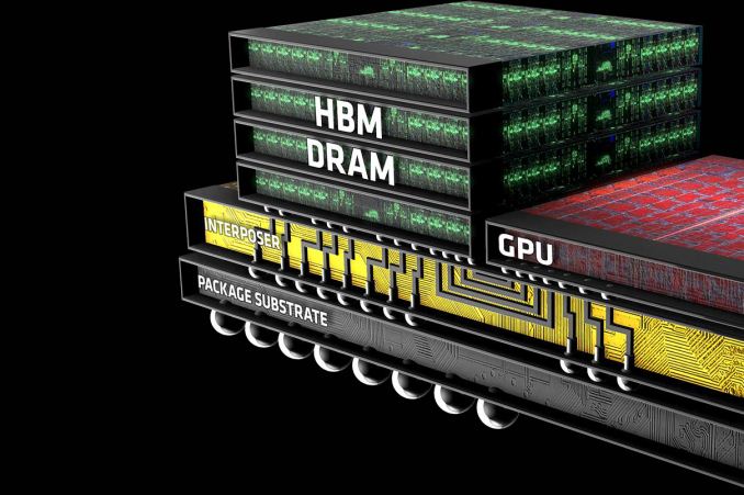
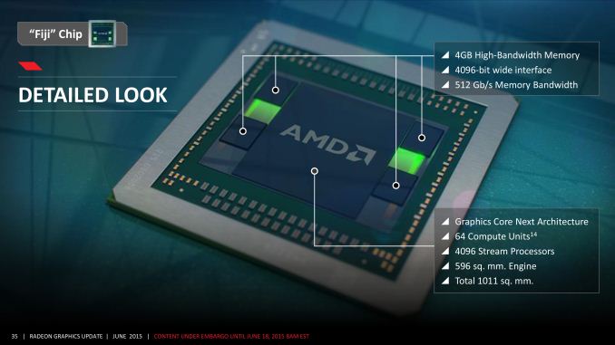
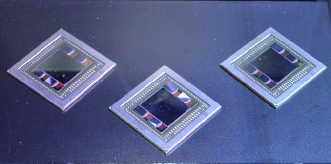
Fiji’s inclusion of High Bandwidth Memory (HBM) technology complicates the picture somewhat when talking about GPUs. Whereas past GPUs were defined by the GPU die itself and then the organic substrate package it sits on, the inclusion of HBM requires a third layer, the silicon interposer. The job of the interposer is to sit between the package and the GPU, serving as the layer that connects the on-package HBM memory stacks with the GPU. Essentially a very large chip without any expensive logic on it, the silicon interposer allows for finer, denser signal routing than organic packaging is capable of, making the ultra-wide 4096-bit HBM bus viable for the first time.
We’ll get to HBM in detail in a bit, but it’s important to call out the impact of HBM and the interposer early, since they have a distinct impact on how Fiji was designed and what its capabilities are.
As for Fiji itself, Fiji is unlike any GPU built before by AMD, and not only due to the use of HBM. More than anything else, it’s simply huge, 596mm2 to be precise. As we mentioned in our introduction, AMD has traditionally shied away from big chips, even after the “small die” era ended, and for good reason. Big chips are expensive to develop, expensive to produce, take longer to develop, and yield worse than small chips (this being especially the case early-on for 40nm). Altogether they’re riskier than smaller chips, and while there are times where they are necessary, AMD has never reached this point until now.
The end result is that for the first time since the unified shader era began, AMD has gone toe-to-toe with NVIDIA on die size. Fiji’s 596mm2 die size is just 5mm2 (<1%) smaller than NVIDIA’s GM200, and more notably still hits TSMC’s 28nm reticle limit. TSMC can’t build chips any bigger than this; Fiji is as big a chip as AMD can order.
| AMD Big GPUs | ||||
| Die Size | Native FP64 Rate | |||
| Fiji (GCN 1.2) | 596mm2 | 1/16 | ||
| Hawaii (GCN 1.1) | 438mm2 | 1/2 | ||
| Tahiti (GCN 1.0) | 352mm2 | 1/4 | ||
| Cayman (VLIW4) | 389mm2 | 1/4 | ||
| Cypress (VLIW5) | 334mm2 | 1/5 | ||
| RV790 (VLIW5) | 282mm2 | N/A | ||
Looking at Fiji relative to AMD’s other big GPUs, it becomes very clear very quickly just how significant this change is for AMD. When Hawaii was released in 2013 at 438mm2, it was already AMD’s biggest GPU ever for its time. And yet Fiji dwarfs it, coming in at 158mm2 (36%) larger. The fact that Fiji comes at the latter-half of the 28nm process’s life time means that such a large GPU is not nearly as risky now as it would have been in 2011/2012 (NVIDIA surely took some licks internally on GK110), but still, nothing else we can show you today can really sell the significance of Fiji to AMD as much as the die size can.
And the fun doesn’t stop there. Along with producing the biggest die they could, AMD has also more or less gone the direction of NVIDIA and Maxwell in the case of Fiji, building what is unambiguously the most gaming/FP32-centric GPU the company could build. With GCN supporting power-of-two FP64 rates between 1/2 and 1/16, AMD has gone for the bare minimum in FP64 performance that their architecture allows, leading to a 1/16 FP64 rate on Fiji. This is a significant departure from Hawaii, which implemented native support for ½ rate, and on consumer parts offered a handicapped 1/8 rate. Fiji will not be a FP64 powerhouse – its 4GB of VRAM is already perhaps too large of a handicap for the HPC market – so instead we get AMD’s best FP32 GPU going against NVIDIA’s best FP32 GPU.
AMD’s final ace up their sleeve on die size is HBM. Along with HBM’s bandwidth and power benefits, HBM is also much simpler to implement, requiring less GPU space for PHYs than GDDR5 does. This is in part due to the fact that HBM stacks have their own logic layer, distributing some of the logic on to each stack, and furthermore a benefit of the fact that the signaling logic that remains doesn’t have to be nearly as complex since the frequencies are so much lower. 4096-bits of HBM PHYs still takes up a fair bit of space – though AMD won’t tell us how much – but it’s notably lower than the amount of space AMD was losing to Hawaii’s GDDR5 memory controllers.
The end result is that not only has AMD built their biggest GPU ever, but they have done virtually everything they can to maximize the amount of die space they get to allocate to FP32 and rendering resources. Simply put, AMD has never reached so high and aimed for parity with NVIDIA in this manner.
Ultimately this puts Fiji’s transistor count at 8.9 billion transistors, even more than the 8 billion transistors found in NVIDIA’s GM200, and, as expected, significantly more than Hawaii’s 6.2 billion. Interestingly enough, on a relative basis this is almost exactly the same increase we saw with Hawaii; Fiji packs in 43.5% more transistors than Hawaii, and Hawaii packed in 43.9% more transistors than Tahiti. So going by transistors alone, Fiji is very much to Hawaii what Hawaii was to Tahiti.
Finally, as large as the Fiji GPU is, the silicon interposer it sits on is even larger. The interposer measures 1011mm2, nearly twice the size of Fiji. Since Fiji and its HBM stacks need to fit on top of it, the interposer must be very large to do its job, and in the process it pushes its own limits. The actual interposer die is believed to exceed the reticle limit of the 65nm process AMD is using to have it built, and as a result the interposer is carefully constructed so that only the areas that need connectivity receive metal layers. This allows AMD to put down such a large interposer without actually needing a fab capable of reaching such a large reticle limit.
What’s interesting from a design perspective is that the interposer and everything on it is essentially the heart and soul of the GPU. There is plenty of power regulation circuitry on the organic package and even more on the board itself, but within the 1011mm2 floorplan of the interposer, all of Fiji’s logic and memory is located. By mobile standards it’s very nearly an SoC in and of itself; it needs little more than external power and I/O to operate.


458 Comments
View All Comments
testbug00 - Sunday, July 5, 2015 - link
You don't need architecture improvements to use DX12/Vulkan/etc. The APIs merely allow you to implement them over DX11 if you choose to. You can write a DX12 game without optimizing for any GPUs (although, not doing so for GCN given consoles are GCN would be a tad silly).If developers are aiming to put low level stuff in whenever they can than the issue becomes that due to AMD's "GCN everywhere" approach developers may just start coding for PS4, porting that code to Xbox DX12 and than porting that to PC with higher textures/better shadows/effects. In which Nvidia could take massive performance deficites to AMD due to not getting the same amount of extra performance from DX12.
Don't see that happening in the next 5 years. At least, not with most games that are console+PC and need huge performance. You may see it in a lot of Indie/small studio cross platform games however.
RG1975 - Thursday, July 2, 2015 - link
AMD is getting there but, they still have a little bit to go to bring us a new "9700 Pro". That card devastated all Nvidia cards back then. That's what I'm waiting for to come from AMD before I switch back.Thatguy97 - Thursday, July 2, 2015 - link
would you say amd is now the "geforce fx 5800"piroroadkill - Thursday, July 2, 2015 - link
Everyone who bought a Geforce FX card should feel bad, because the AMD offerings were massively better. But now AMD is close to NVIDIA, it's still time to rag on AMD, huh?That said, of course if I had $650 to spend, you bet your ass I'd buy a 980 Ti.
Thatguy97 - Thursday, July 2, 2015 - link
oh believe me i remember they felt bad lol but im not ragging on amd but nvidia stole their thunder with the 980 tiKateH - Thursday, July 2, 2015 - link
C'mon, Fury isn't even close to the Geforce FX level of fail. It's really hard to overstate how bad the FX5800 was, compared to the Radeon 9700 and even the Geforce 4600Ti.The Fury X wins some 4K benchmarks, the 980Ti wins some. The 980Ti uses a bit less power but the Fury X is cooler and quieter.
Geforce FX level of fail would be if the Fury X was released 3 months from now to go up against the 980Ti with 390X levels of performance and an air cooler.
Thatguy97 - Thursday, July 2, 2015 - link
To be fair the 5950 ultra was actually decentMorawka - Thursday, July 2, 2015 - link
your understating nvidia's scores.. the won 90% of all benchmarks, not just "some". a full 120W more power under furmark load and they are using HBM!!looncraz - Thursday, July 2, 2015 - link
Furmark power load means nothing, it is just a good way to stress test and see how much power the GPU is capable of pulling in a worst-case scenario and how it behaves in that scenario.While gaming, the difference is miniscule and no one will care one bit.
Also, they didn't win 90% of the benchmarks at 4K, though they certainly did at 1440. However, the real world isn't that simple. A 10% performance difference in GPUs may as well be zero difference, there are pretty much no game features which only require a 10% higher performance GPU to use... or even 15%.
As for the value argument, I'd say they are about even. The Fury X will run cooler and quieter, take up less space, and will undoubtedly improve to parity or beyond the 980Ti in performance with driver updates. For a number of reasons, the Fury X should actually age better, as well. But that really only matters for people who keep their cards for three years or more (which most people usually do). The 980Ti has a RAM capacity advantage and an excellent - and known - overclocking capacity and currently performs unnoticeably better.
I'd also expect two Fury X cards to outperform two 980Ti cards with XFire currently having better scaling than SLI.
chizow - Thursday, July 2, 2015 - link
The differences in minimums aren't miniscule at all, and you also seem to be discounting the fact 980Ti overclocks much better than Fury X. Sure XDMA CF scales better when it works, but AMD has shown time and again, they're completely unreliable for timely CF fixes for popular games to the point CF is clearly a negative for them right now.