AMD Dives Deep On High Bandwidth Memory - What Will HBM Bring AMD?
by Ryan Smith on May 19, 2015 8:40 AM ESTHBM: Wide & Slow Makes It Fast
Given the challenges faced in pushing GDDR5 and similar memory technologies even further, development of high bandwidth memory technology has in the last decade shifted back towards wider, slower interfaces. As serial interfaces reach their limits, parallel interfaces become an increasingly viable alternative. And although they bring with them their own challenges – there’s a reason serial interfaces have been dominant most recently, after all – the ramp up of challenges in further improving serial interfaces has coincided with the development of technologies that make parallel interfaces easier to implement. As a result the pendulum has swung back to parallel interfaces and HBM.
HBM in a nutshell takes the wide & slow paradigm to its fullest. Rather than building an array of high speed chips around an ASIC to deliver 7Gbps+ per pin over a 256/384/512-bit memory bus, HBM at its most basic level involves turning memory clockspeeds way down – to just 1Gbps per pin – but in exchange making the memory bus much wider. How wide? That depends on the implementation and generation of the specification, but the examples AMD has been showcasing so far have involved 4 HBM devices (stacks), each featuring a 1024-bit wide memory bus, combining for a massive 4096-bit memory bus. It may not be clocked high, but when it’s that wide, it doesn’t need to be.
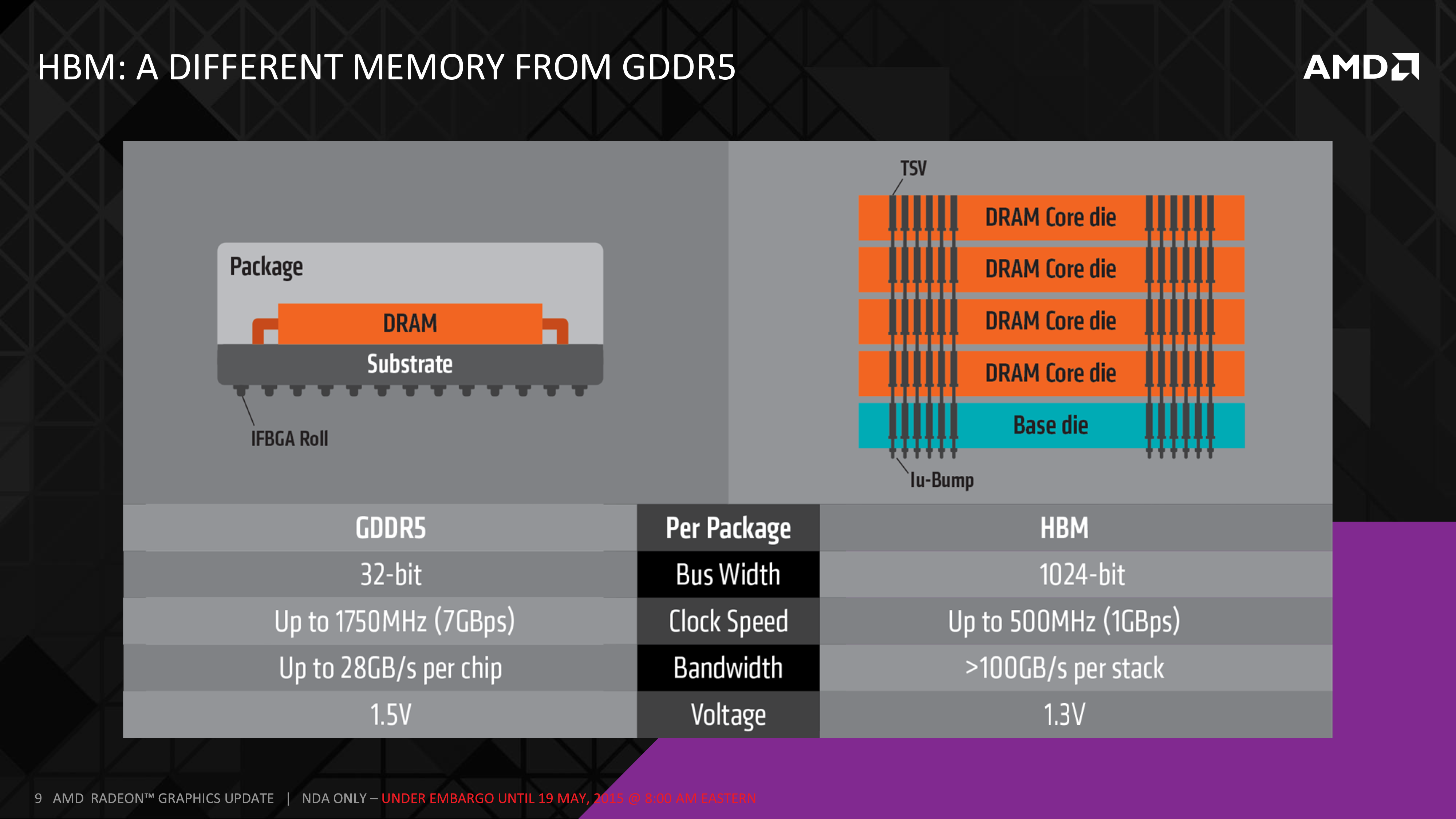
Of course while extra memory bandwidth is nice, the far more interesting part is how HBM delivers this. Although the idea of a wide, slow parallel bus is easy enough to comprehend on paper, implementing it is a whole other matter. A 4096-bit memory bus involves thousands of traces, far more than GDDR5, all of which must be carefully constructed in order to make HBM work. As a result there are a couple of fundamental technologies that are seeing their big (though not necessarily initial) introduction with HBM.
The first and most fundamental matter is how do you efficiently route a 4096-bit memory bus? Even the best surface mounting BGA technologies have their limits, and as it is Hawaii was pushing things with its 512-bit GDDR5 memory bus. An even wider bus only makes that harder, inviting issues both with the routing such a wide bus on a PCB or chip substrate, and in using BGA to connect a chip to those traces.
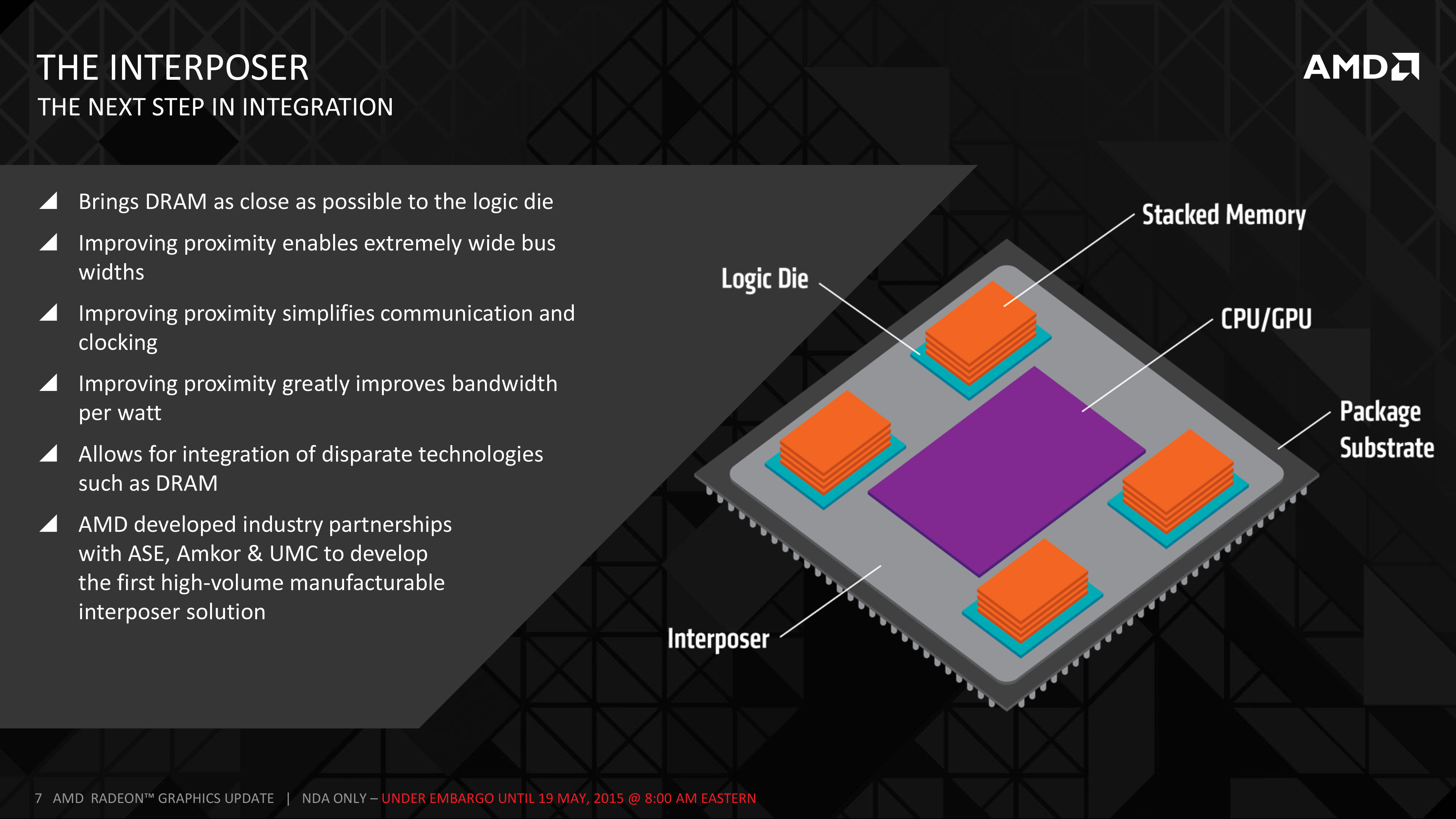
First part of the solution to that in turn was to develop something capable of greater density routing, and that something was the silicon interposer. The interposer in its broadest terms is a partially fabbed silicon chip that instead of being developed into a full ASIC packed with logic, is only developed as far as having metal layers, in order to route signals and power among devices. The interposer in turn works because it exploits some of the core advantages of modern photolithographic processes, allowing for very fine paths to be created that would otherwise not be possible/practical on traditional PCBs and substrates.
Using a silicon interposer solves some of the fundamental problems with HBM, but it also provides some ancillary benefits as well. Along with solving the obvious routing issue, the interposer allows for DRAM to be placed very close to an ASIC, but without being placed on top of it (ala Package-on-package), which is impractical for high TDP devices like GPUs. By being able to place DRAM so close to the ASIC, it avoids the drawbacks of long memory paths, making the shorter paths both simpler to construct and require less power in the process. It also benefits integration, as similar to PoP technology, you can have more of the device’s functionality located on the same package as the ASIC, reducing the number of devices that need to be placed off-package and routed to the ASIC.
Of course the interposer does come with a drawback as well, and that’s cost. While AMD is not talking about costs in great detail – this is a technology deep dive, not an analyst meeting – the fact that the interposer is essentially a very large, partially developed silicon chip means that it’s relatively expensive to produce, especially compared to the very low costs of PCBs and traditional substrates. Mitigating this is the fact that interposers don’t need to go through the most complex and expensive phases of photolithography – the actual front-end lithography – so the cost is only the silicon wafer itself, along with the work required to create the metal layers, with the final interposer only being some 100 microns thick. Furthermore this doesn’t require cutting-edge fabs – old, fully amortized 65nm equipment works quite well – which further keeps the costs down. The end result is that the interposer is still a significant cost, but it is not as bad as it initially seems. This ultimately is why HBM will first be introduced on high margin products like high-end video cards before potentially making its way down to cheaper devices like APUs.
Meanwhile AMD and their vendors will over the long run also benefit from volume production. The first interposers are being produced on retooled 65nm lithographic lines, however once volume production scales up, it will become economical to develop interposer-only lines that are cheaper to operate since they don’t need the ability to offer full lithography as well. Where that cut-off will be is not quite clear at this time, though it sounds like it will happen sooner than later.
Looking at the broader picture, in the grand scheme of things the interposer becomes a new layer on a complete chip, sitting between the traditional substrate and any DRAM/ASICs mounted on top of it. Microbumps will connect the DRAM and ASICs to the interposer, and the interposer will then be connected to the substrate, before finally the substrate is connected to its partner PCB. PCB mounting itself will become a bit easier in the process, as there’s no longer a need to route memory traces through the substrate, which means the only remaining connections are data (PCIe bus, etc) and power for the ASIC and DRAM. All the complex routing is essentially localized to occurring at the interposer layer.
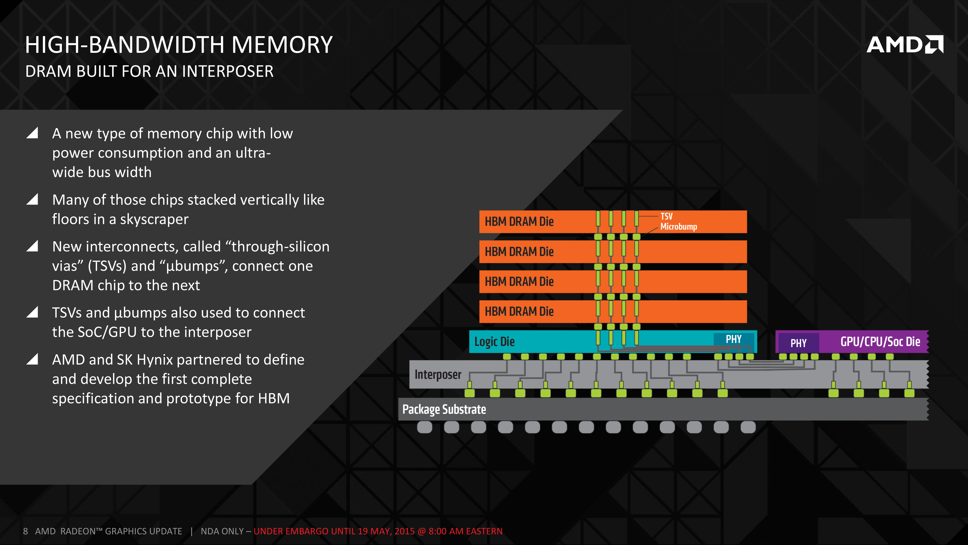
Moving on, the other major technological breakthrough here is the creation of through-silicon vias (TSVs). With the interposer to enable the routing of a dense memory bus, the other issue to solve was the creation of dense memory. The solution to this was to stack multiple memory dies together into a single device/stack, in order to create the single 1024-bit stack, and TSVs are in turn what make this possible.
The reason for stacking DRAM is pretty straightforward: it makes production easier by reducing the DRAM to fewer discrete devices, not to mention it saves space. The challenge here is that you can’t have traditional surface mount connections since the DRAM is stacked, and traditional edge connections (as used in PoP) are neither dense enough nor do they scale well to the kind of stacks HBM would require.

TSVs. Image Courtesy The International Center for Materials Nanoarchitectonics
As a result a means was needed to route DRAM connections though the lower layers of the stack, and this problem was solved with TSVs. Whereas regular vias offer the ability to connect two layers together, TSVs extend this principle by running the vias straight through silicon devices in order to connect layers farther out. The end result is something vaguely akin to DRAM dies surface mounted on top of each other via microbumps, but with the ability to communicate through the layers. From a manufacturing standpoint, between the silicon interposer and TSVs, TSVs are the more difficult technology to master as it essentially combines all the challenges of DRAM fabbing with the challenges of stacking those DRAM dies on top of each other.
Having developed the means to stack DRAM, the final component of an HBM stack is a logic die that lies on the bottom of the stack. Similarly outfitted with TSVs, the logic die is responsible for actually operating the DRAM dies above it, and then handling the operation of the HBM bus between the stack and the ASIC. This actually ends up being a rather interesting development since the net result is more logic added despite the simplicity of the HBM bus, but at the same time thanks to TSVs and the interposer, it’s easier than ever to add that logic.


163 Comments
View All Comments
ravyne - Tuesday, May 19, 2015 - link
No, not necessarily. AMD isn't exactly allaying any fears by remaining silent so far, but there's a method for chaining two HBM chips together, similar to how chip-select works in normal DDR RAM or SRAMs in embedded systems -- basically you have two chips sharing that 1024-bit memory bus, but there's a separate control signal that indicates which chip the host is talking to. In theory you can chain things along forever with enough chip selects, but a high-performance and highly-parallel bus like HBM is practically limited by signal-propagation latency and misalignment, so using just two chips per HBM bus is more of a practical limitation.looncraz - Tuesday, May 19, 2015 - link
Nope, at least not according to my understanding. In fact, in theory, HBM1 can be configured, at reduced speeds, at well over 8GB. The article even mentions a technical bit of information pertaining to this:"HBM in turn allows from 2 to 8 stacks to be used, with each stack carrying 1GB of DRAM."
From 2GB to 8GB right there, without any trickery. It appears HBM chips need to be used in pairs (otherwise a 2 chip minimum makes no sense), and likely needs to be addressed in pairs (with a 512-bit bus per chip, it would seem). This would indicate there is a two-bit address line which allows from one to four pairs to be individually addressed, or perhaps four binary address lines, whichever they deemed to be more economical and prudent. Either way it appears each stack has a 512-bit data bus.
If correct, you can even use a single 1024-bit bus and interleave on the bus and address 8GB @ 128GB/s maximum. A 2048-bit bus would limit at 16GB @ 256 GB/s, a 3072-bit bus could use 24GB @ 384GB/s, and a 4096-bit bus could use 32GB @ 512GB/s. Interleaving on the bus, though, would increase latency and decrease throughput.
That said, no company, especially not AMD, would design and then bet big on a memory technology that limited them to 4GB without having a solution ready. Everything I mentioned that the HBM chips would be required to support are standard for memory chips made for the last many many decades and was probably included even in the first rough draft for the command protocol without anyone even thinking about it twice. That's just how it works.
It might even be possible to use an 512-bit bus and some latching circuitry to drive HBM. You might even be able to do this with good performance and high capacities without modifying the memory chips at all.
chizow - Wednesday, May 20, 2015 - link
All sounds really good in theory, unfortunately none of the (substantial) source material from AMD/Hynix supports this, nor do the comments from the AMD VP Macri who seems more or less resigned to the fact AMD is going forward with 4GB for HBM1.But in any case, hopefully you won't be too disappointed if it is only 4GB.
looncraz - Wednesday, May 20, 2015 - link
Your comment made me remember that the standard was submitted to JEDEC.JESD235 pertains to HBM (v1), from it I was able to determine that if 8GB was to be supported using 1GB stacks the command interface would have to be duplicated per chip, but the (much larger) data bus could be shared - with some important timing caveats, of course, but that is nothing new for memory controllers (in fact, that is most of what they do), but it is not necessarily something you'd want to do without having already had a working product using the memory technology... and certainly not something you'd bother implementing if you expected higher capacity chips to be available in a year's time...
I finally see how HBM works internally (something that's been lacking from most "technical" articles), and I see why its external interface doesn't follow convention - it's basically an 8/16 bank "up to 8 channel" collection of DRAM chips. Each channel can be addressed separately with a 128-bit data bus and can support 32Gb (4GB) of DRAM.
So HBM uses the relevant addressing lines internally, if at all (vendor specific), and doesn't provide for such a mechanism externally.
From what I'm seeing, it would seem you can build HBM with any width you want, in intervals of 128-bits. Of course, standards are designed to be flexible. That could mean lower powered devices could use 256bit HBM interfaces to save power... unless I'm totally missing something (which is quite likely, it isn't like reading a standards document is the same as reading a quick overview ;-)).
chizow - Thursday, May 21, 2015 - link
Yep exactly, that's where the original 4GB limits for HBM1 came from originally, the JEDEC/Hynix source documents.akamateau - Thursday, May 28, 2015 - link
With Highbandwidth memory depth is not necessary. Of course only the benchmarks will actually show us.And of course DX11 will be useless for this product. HBM was designed to solve a problem! DX12 solves the CPU bottleneck however DX12 benchmarks shows that performance scale sup nicely to 20MILLION + draw calls per second with 6 CPU cores feeding the GPU. When the CPU has 8 coress the performance flatlines and does not get anybetter.
ANAND demonstrated this quite clearly a few weeks back. However HBM will scael far beyond 6 cores as their is more through-put.
Of course that would mean that 390x must be benched using DX12 benchmarks. But that is what they were designed for: Mantle and DX12
akamateau - Thursday, May 28, 2015 - link
You do not need the memory depth with HBM.HBM was designed to solve a problem that becomes apparent with DX12. DX11 does not support multithreaded and multicore gaming. DX12 enables ALL CPU cores to feed the GPU through Asynchronous Shader Pipelines and Asynchronous Compute Engines.
With DX12 GPU performance scales well to 6 cpu cores, beyond that and the GPU drawcall perfomance flatlines: GPU bottleneck. HBM will solve this problem.
DX11 is such a crippling API that anyone even using it to make a decision regarding a $1000 GPU purchase will lkely waste their money.
With DX12 Benching Radeon 390x with HBM will demostrate 400-500% performance increases over DX11.
Do you want to know the facts before you spend your money? Then demand DX12 benchmarks!!
akamateau - Thursday, May 28, 2015 - link
According to AMD's Joe Macri, GDDR5 fed GPUs actually have too much unused memory today. Because to increase GPU memory bandwidth, wider memory interfaces are used. And because wider memory interfaces require a larger amount of GDDR5 memory chips, GPUs ended up with more memory capacity than is actually needed.Macri also stated that AMD invested a lot into improving utilization of the frame buffer. This could include on-die memory compression techniques which are integrated into the GPU hardware itself. Or more clever algorithms on the driver level."http://wccftech.com/amd-addresses-capacity-limitat...
DX11 will not likely allow an HBM AIB to show much of an improvement in performance. Run DX12 games or benchmarks and HBM will rock that AIB!
akamateau - Thursday, May 28, 2015 - link
You do not need the memory depth with HBM.HBM was designed to solve a problem that becomes apparent with DX12. DX11 does not support multithreaded and multicore gaming. DX12 enables ALL CPU cores to feed the GPU through Asynchronous Shader Pipelines and Asynchronous Compute Engines.
With DX12 GPU performance scales well to 6 cpu cores, beyond that and the GPU drawcall perfomance flatlines: GPU bottleneck. HBM will solve this problem.
DX11 is such a crippling API that anyone even using it to make a decision regarding a $1000 GPU purchase will lkely waste their money.
With DX12 Benching Radeon 390x with HBM will demostrate 400-500% performance increases over DX11.
Do you want to know the facts before you spend your money? Then demand DX12 benchmarks!!
A5 - Tuesday, May 19, 2015 - link
Interesting. The article says that AMD is the only anticipated user of HBM1, but are there any rumors on where HBM2 might go?Obvious thing is to make the stacks higher/denser (2-4GB per stack seems more suited to high-end 4K/VR gaming) and increasing the clocks on the interface.