AMD Dives Deep On High Bandwidth Memory - What Will HBM Bring AMD?
by Ryan Smith on May 19, 2015 8:40 AM ESTHistory: Where GDDR5 Reaches Its Limits
To really understand HBM we’d have to go all the way back to the first computer memory interfaces, but in the interest of expediency and sanity, we’ll condense that lesson down to the following. The history of computer and memory interfaces is a consistent cycle of moving between wide parallel interfaces and fast serial interfaces. Serial ports and parallel ports, USB 2.0 and USB 3.1 (Type-C), SDRAM and RDRAM, there is a continual process of developing faster interfaces, then developing wider interfaces, and switching back and forth between them as conditions call for.
So far in the race for PC memory, the pendulum has swung far in the direction of serial interfaces. Though 4 generations of GDDR, memory designers have continued to ramp up clockspeeds in order to increase available memory bandwidth, culminating in GDDR5 and its blistering 7Gbps+ per pin data rate. GDDR5 in turn has been with us on the high-end for almost 7 years now, longer than any previous memory technology, and in the process has gone farther and faster than initially planned.
But in the cycle of interfaces, the pendulum has finally reached its apex for serial interfaces when it comes to GDDR5. Back in 2011 at an AMD video card launch I asked then-graphics CTO Eric Demers about what happens after GDDR5, and while he expected GDDR5 to continue on for some time, it was also clear that GDDR5 was approaching its limits. High speed buses bring with them a number of engineering challenges, and while there is still headroom left on the table to do even better, the question arises of whether it’s worth it.

AMD 2011 Technical Forum and Exhibition
The short answer in the minds of the GPU community is no. GDDR5-like memories could be pushed farther, both with existing GDDR5 and theoretical differential I/O based memories (think USB/PCIe buses, but for memory), however doing so would come at the cost of great power consumption. In fact even existing GDDR5 implementations already draw quite a bit of power; thanks to the complicated clocking mechanisms of GDDR5, a lot of memory power is spent merely on distributing and maintaining GDDR5’s high clockspeeds. Any future GDDR5-like technology would only ratchet up the problem, along with introducing new complexities such as a need to add more logic to memory chips, a somewhat painful combination as logic and dense memory are difficult to fab together.
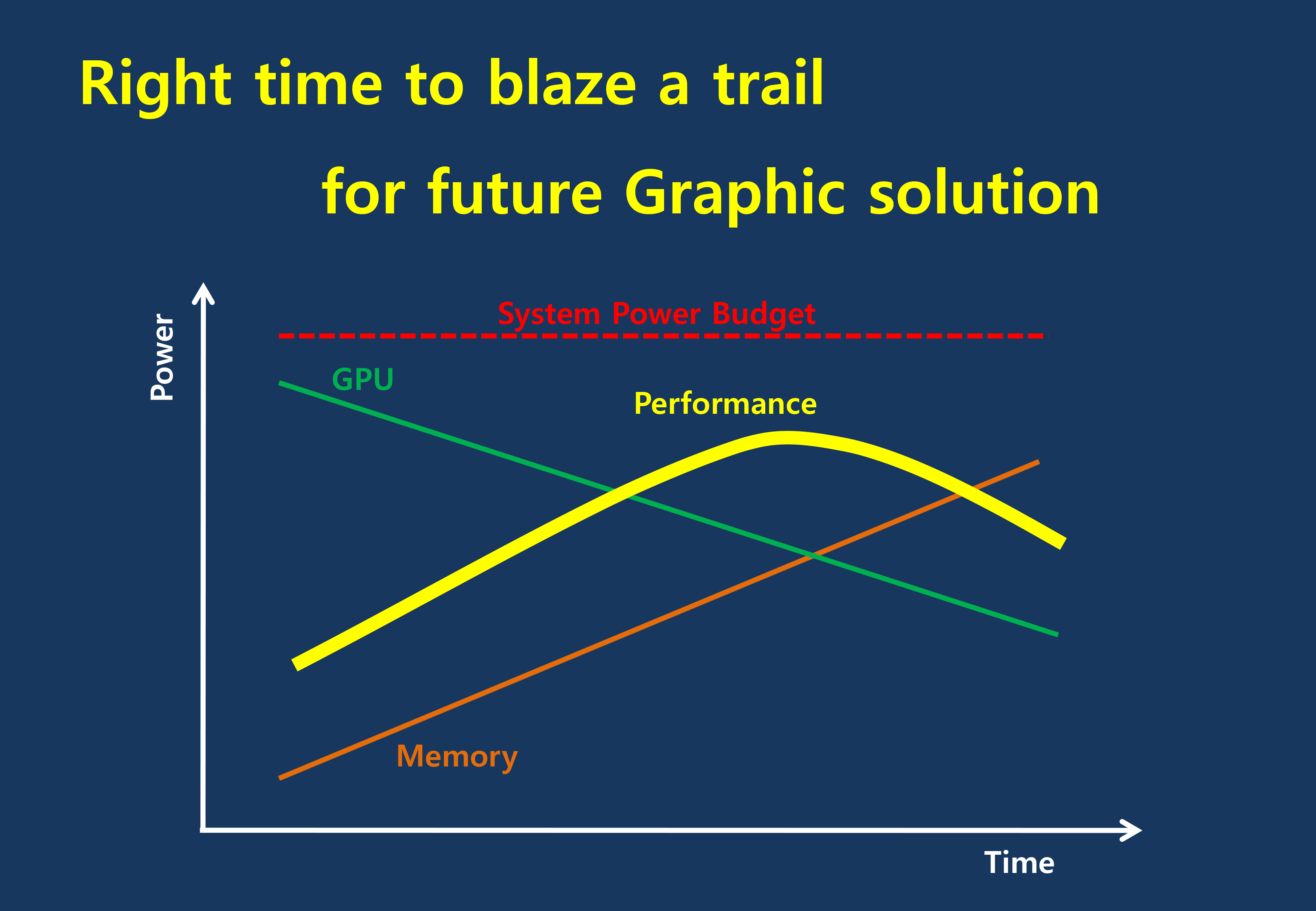
The current GDDR5 power consumption situation is such that by AMD’s estimate 15-20% of Radeon R9 290X’s (250W TDP) power consumption is for memory. This being even after the company went with a wider, slower 512-bit GDDR5 memory bus clocked at 5GHz as to better contain power consumption. So using a further, faster, higher power drain memory standard would only serve to exacerbate that problem.
All the while power consumption for consumer devices has been on a downward slope as consumers (and engineers) have made power consumption an increasingly important issue. The mobile space, with its fixed battery capacity, is of course the prime example, but even in the PC space power consumption for CPUs and GPUs has peaked and since come down some. The trend is towards more energy efficient devices – the idle power consumption of a 2005 high-end GPU would be intolerable in 2015 – and that throws yet another wrench into faster serial memory technologies, as power consumption would be going up exactly at the same time as overall power consumption is expected to come down, and individual devices get lower power limits to work with as a result.
Finally, coupled with all of the above has been issues with scalability. We’ll get into this more when discussing the benefits of HBM, but in a nutshell GDDR5 also ends up taking a lot of space, especially when we’re talking about 384-bit and 512-bit configurations for current high-end video cards. At a time when everything is getting smaller, there is also a need to further miniaturize memory, something that GDDR5 and potential derivatives wouldn’t be well suited to resolve.
The end result is that in the GPU memory space, the pendulum has started to swing back towards parallel memory interfaces. GDDR5 has been taken to the point where going any further would be increasingly inefficient, leading to researchers and engineers looking for a wider next-generation memory interface. This is what has led them to HBM.


163 Comments
View All Comments
ravyne - Tuesday, May 19, 2015 - link
No, not necessarily. AMD isn't exactly allaying any fears by remaining silent so far, but there's a method for chaining two HBM chips together, similar to how chip-select works in normal DDR RAM or SRAMs in embedded systems -- basically you have two chips sharing that 1024-bit memory bus, but there's a separate control signal that indicates which chip the host is talking to. In theory you can chain things along forever with enough chip selects, but a high-performance and highly-parallel bus like HBM is practically limited by signal-propagation latency and misalignment, so using just two chips per HBM bus is more of a practical limitation.looncraz - Tuesday, May 19, 2015 - link
Nope, at least not according to my understanding. In fact, in theory, HBM1 can be configured, at reduced speeds, at well over 8GB. The article even mentions a technical bit of information pertaining to this:"HBM in turn allows from 2 to 8 stacks to be used, with each stack carrying 1GB of DRAM."
From 2GB to 8GB right there, without any trickery. It appears HBM chips need to be used in pairs (otherwise a 2 chip minimum makes no sense), and likely needs to be addressed in pairs (with a 512-bit bus per chip, it would seem). This would indicate there is a two-bit address line which allows from one to four pairs to be individually addressed, or perhaps four binary address lines, whichever they deemed to be more economical and prudent. Either way it appears each stack has a 512-bit data bus.
If correct, you can even use a single 1024-bit bus and interleave on the bus and address 8GB @ 128GB/s maximum. A 2048-bit bus would limit at 16GB @ 256 GB/s, a 3072-bit bus could use 24GB @ 384GB/s, and a 4096-bit bus could use 32GB @ 512GB/s. Interleaving on the bus, though, would increase latency and decrease throughput.
That said, no company, especially not AMD, would design and then bet big on a memory technology that limited them to 4GB without having a solution ready. Everything I mentioned that the HBM chips would be required to support are standard for memory chips made for the last many many decades and was probably included even in the first rough draft for the command protocol without anyone even thinking about it twice. That's just how it works.
It might even be possible to use an 512-bit bus and some latching circuitry to drive HBM. You might even be able to do this with good performance and high capacities without modifying the memory chips at all.
chizow - Wednesday, May 20, 2015 - link
All sounds really good in theory, unfortunately none of the (substantial) source material from AMD/Hynix supports this, nor do the comments from the AMD VP Macri who seems more or less resigned to the fact AMD is going forward with 4GB for HBM1.But in any case, hopefully you won't be too disappointed if it is only 4GB.
looncraz - Wednesday, May 20, 2015 - link
Your comment made me remember that the standard was submitted to JEDEC.JESD235 pertains to HBM (v1), from it I was able to determine that if 8GB was to be supported using 1GB stacks the command interface would have to be duplicated per chip, but the (much larger) data bus could be shared - with some important timing caveats, of course, but that is nothing new for memory controllers (in fact, that is most of what they do), but it is not necessarily something you'd want to do without having already had a working product using the memory technology... and certainly not something you'd bother implementing if you expected higher capacity chips to be available in a year's time...
I finally see how HBM works internally (something that's been lacking from most "technical" articles), and I see why its external interface doesn't follow convention - it's basically an 8/16 bank "up to 8 channel" collection of DRAM chips. Each channel can be addressed separately with a 128-bit data bus and can support 32Gb (4GB) of DRAM.
So HBM uses the relevant addressing lines internally, if at all (vendor specific), and doesn't provide for such a mechanism externally.
From what I'm seeing, it would seem you can build HBM with any width you want, in intervals of 128-bits. Of course, standards are designed to be flexible. That could mean lower powered devices could use 256bit HBM interfaces to save power... unless I'm totally missing something (which is quite likely, it isn't like reading a standards document is the same as reading a quick overview ;-)).
chizow - Thursday, May 21, 2015 - link
Yep exactly, that's where the original 4GB limits for HBM1 came from originally, the JEDEC/Hynix source documents.akamateau - Thursday, May 28, 2015 - link
With Highbandwidth memory depth is not necessary. Of course only the benchmarks will actually show us.And of course DX11 will be useless for this product. HBM was designed to solve a problem! DX12 solves the CPU bottleneck however DX12 benchmarks shows that performance scale sup nicely to 20MILLION + draw calls per second with 6 CPU cores feeding the GPU. When the CPU has 8 coress the performance flatlines and does not get anybetter.
ANAND demonstrated this quite clearly a few weeks back. However HBM will scael far beyond 6 cores as their is more through-put.
Of course that would mean that 390x must be benched using DX12 benchmarks. But that is what they were designed for: Mantle and DX12
akamateau - Thursday, May 28, 2015 - link
You do not need the memory depth with HBM.HBM was designed to solve a problem that becomes apparent with DX12. DX11 does not support multithreaded and multicore gaming. DX12 enables ALL CPU cores to feed the GPU through Asynchronous Shader Pipelines and Asynchronous Compute Engines.
With DX12 GPU performance scales well to 6 cpu cores, beyond that and the GPU drawcall perfomance flatlines: GPU bottleneck. HBM will solve this problem.
DX11 is such a crippling API that anyone even using it to make a decision regarding a $1000 GPU purchase will lkely waste their money.
With DX12 Benching Radeon 390x with HBM will demostrate 400-500% performance increases over DX11.
Do you want to know the facts before you spend your money? Then demand DX12 benchmarks!!
akamateau - Thursday, May 28, 2015 - link
According to AMD's Joe Macri, GDDR5 fed GPUs actually have too much unused memory today. Because to increase GPU memory bandwidth, wider memory interfaces are used. And because wider memory interfaces require a larger amount of GDDR5 memory chips, GPUs ended up with more memory capacity than is actually needed.Macri also stated that AMD invested a lot into improving utilization of the frame buffer. This could include on-die memory compression techniques which are integrated into the GPU hardware itself. Or more clever algorithms on the driver level."http://wccftech.com/amd-addresses-capacity-limitat...
DX11 will not likely allow an HBM AIB to show much of an improvement in performance. Run DX12 games or benchmarks and HBM will rock that AIB!
akamateau - Thursday, May 28, 2015 - link
You do not need the memory depth with HBM.HBM was designed to solve a problem that becomes apparent with DX12. DX11 does not support multithreaded and multicore gaming. DX12 enables ALL CPU cores to feed the GPU through Asynchronous Shader Pipelines and Asynchronous Compute Engines.
With DX12 GPU performance scales well to 6 cpu cores, beyond that and the GPU drawcall perfomance flatlines: GPU bottleneck. HBM will solve this problem.
DX11 is such a crippling API that anyone even using it to make a decision regarding a $1000 GPU purchase will lkely waste their money.
With DX12 Benching Radeon 390x with HBM will demostrate 400-500% performance increases over DX11.
Do you want to know the facts before you spend your money? Then demand DX12 benchmarks!!
A5 - Tuesday, May 19, 2015 - link
Interesting. The article says that AMD is the only anticipated user of HBM1, but are there any rumors on where HBM2 might go?Obvious thing is to make the stacks higher/denser (2-4GB per stack seems more suited to high-end 4K/VR gaming) and increasing the clocks on the interface.