Samsung SSD 850 EVO (120GB, 250GB, 500GB & 1TB) Review
by Kristian Vättö on December 8, 2014 10:00 AM ESTThree Bits and Three Dimensions: What's the Deal?
I've covered 3D NAND and TLC NAND in detail in the past and in this article I'll just explain what 3D technology means to TLC NAND and vice versa, so head over to the links above if you are in the search for a deeper analysis of the two technologies.

Truth to be told, 3D technology is ideal for TLC. The fundamental problem of TLC NAND has always been the limited endurance and performance, which is caused by the additional voltage states that are needed to store three bits (i.e. eight possible bit outputs) in one cell. With eight voltage states compared to four in MLC, TLC NAND is less resistant to wear out because it takes a smaller change in the cell charge to corrupt the cell value. Due to the way NAND works, the cells (or the insulators in the cell to be exact) wear out over time, which induces electron leakage that alters the cell charge and hence the voltage state. This gets worse with die shrinks because the number of electrons decreases, making the NAND even less tolerant to wear out.
The key aspect of 3D V-NAND is the process node. By going back to 40nm lithography, the number of electrons increase exponentially, which makes TLC a much more viable technology than it was with modern planar NAND. Obviously, V-NAND doesn't change the basics of TLC NAND because it still takes eight voltage states to differentiate all the possible 3-bit outputs, but thanks to the increased number of electrons there is more breathing room between the states and thus the cells are more error tolerant.

Samsung claims 10x reduction in voltage state overlaps, which is a massive change for the better. You can see how crammed the planar TLC voltage states are, so it's no wonder that the endurance is low because the states are practically overlapping at each point in the voltage distribution and hence even tiny changes in the cell voltage can alter the cell's voltage state.
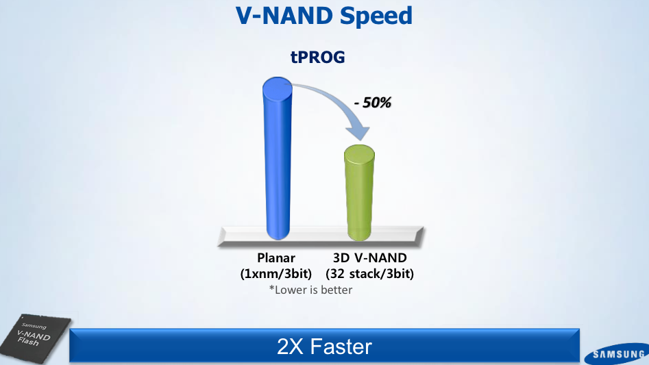
The larger cell structure also enables higher performance because it takes less iterations to program a cell. With planar TLC NAND it took multiple very high voltage pulses as well as numerous verification process to reach the right charge, but with looser voltage distribution the programming process has less steps and thus takes less time.
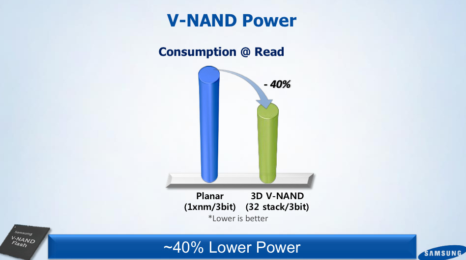
And given the lower read/program latencies and less need for error correction, the power consumption is also considerably lower.
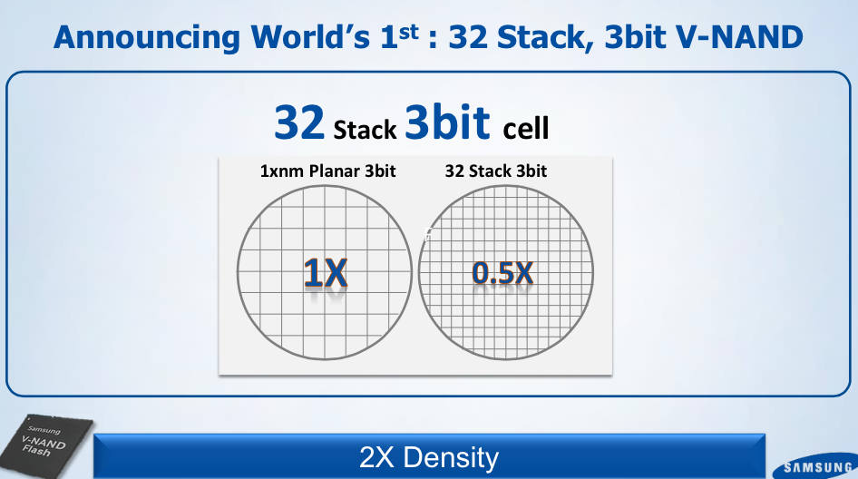
In addition to better latency and power consumption characteristics, Samsung claims doubled the density over its 19nm planar TLC NAND, but without knowing the die size of 128Gbit 32-layer TLC V-NAND, it's hard to say how accurate this is. There have been some whispering that the 128Gbit die would actually be identical to the 86Gbit MLC die because 86Gbit multiplied by 1.5 equals 129Gbit and at the silicon level MLC and TLC aren't any different, but for now that's just speculation.
What I do know is that Samsung started the mass production of TLC V-NAND later, which suggests that the two aren't completely uniform. Moreover, from what I know TLC NAND requires some changes to the peripheral circuitry in order to read three bits from one cell, so while the NAND memory arrays could be alike the die size is still likely at least slightly different. Anyway, we'll find out when Chipworks (or some other silicon analysis company) takes a closer look at the NAND die itself.


97 Comments
View All Comments
Kevin G - Monday, December 8, 2014 - link
They do seem a little low but we just got out of a major sale spree. During the Black Friday/Cyber Monday shopping fest the 480 GB Intel 730 was going for $200. I would have picked up one up myself at that price but they ran out of stock.HisDivineOrder - Wednesday, December 10, 2014 - link
You'd have been better served with the Sandisk Extreme Pro 480GB for $185.davolfman - Monday, December 8, 2014 - link
OCZ's firmware for the Barefoot3 series of chips the ARC100 uses has a less then stellar reputation. Things like unexpected power loss have been known to put it into a state of progressive corruption only recoverable by secure erase. There have been patches that claim to fix this on my Vector (that probably got applied to the ARC out the door), but I haven't seen anyone test if they're working.Oxford Guy - Wednesday, December 31, 2014 - link
Up to its old tricks, then.Kristian Vättö - Tuesday, December 9, 2014 - link
As listed on the table, the prices were taken on December 7 and were accurate at the time.sheh - Monday, December 8, 2014 - link
Can anyone explain the large discrepancy (not only in this case) in sequential speed between Iometer and AS-SSD?Kristian Vättö - Tuesday, December 9, 2014 - link
It's because of TurboWrite. Iometer is a time based tool and the sequential tests are run for one minute, which means that the TurboWrite buffer will be filled and thus the performance goes down as data is written to the TLC array. AS-SSD, on the other hand, only writes a gigabyte of data so it all gets written to the fast SLC cache.sheh - Friday, December 12, 2014 - link
Thanks. I'll have to reread older reviews, but I think there's a similar behavior also on other drives that do not have a fast temporary buffer?maecenas - Monday, December 8, 2014 - link
I saw the 840 EVO 500gb going for $180 over the black Friday - cyber Monday period. It'll interesting to see if Samsung keep the 840 EVO on the market as a the low end, so the 850 EVO can fill the mid-range portion of the market while the 850 Pro serves the high end.Laststop311 - Monday, December 8, 2014 - link
Prices are kinda crappy. Why go with an 850 evo when u can spend 20-30 dollars more and get an 850 pro?