ARM’s Mali Midgard Architecture Explored
by Ryan Smith on July 3, 2014 11:00 AM ESTTechnical Comparisons
As has quickly become tradition for us, to close out our look at the Midgard architecture we want to spend a bit of time comparing it to other SoC GPU architectures. As this is not a performance or benchmark article we aren’t going to dwell on the subject too much, but we find it’s helpful to get a high level overview of theoretical performance.
To do this we’ll take a quick look at theoretical performance for FP32 FLOPS, along with pixel and texel throughput. As this is a purely theoretical comparison it doesn’t (and can’t) take into account architectural efficiency, nor can it take into account real-world clockspeeds. But none the less it gives us something of a baseline.
To that end we asked ARM what a reasonable high-end Mali-T760 configuration might look like. T760 can scale up to 16 shader cores, but as we’ve seen in these scalable designs it’s very rare for anyone to build a SoC that actually takes the number of cores up to the architecture’s limit. And since T760 was only released to customers back in October of 2013, there are only a handful of designs announced so far and none of them are particularly high-end. To that end ARM suggested that a Mali-T760 MP10 would be a reasonable approximation of a high-end shipping configuration, so that is what we’ve gone with.
| GPU Specification Comparison | ||||||
| NVIDIA K1 | Imagination PVR GX6650 | ARM Mali-T760 MP10 | AMD A4-1350 | |||
| FP32 ALUs | 192 | 192 | 100 | 128 | ||
| FP32 FLOPs | 384 | 384 | 200 (340) | 256 | ||
| Pixels/Clock (ROPs) | 4 | 12 | 10 | 4 | ||
| Texels/Clock | 8 | 12 | 10 | 8 | ||
| GFLOPS @ 300MHz | 115.2 GFLOPS | 115.2 GFLOPS | 60 (102) GFLOPS | 76.8 GFLOPS | ||
| Architecture | Kepler | Rogue (6XT) | Midgard (T700) | GCN 1.1 | ||
Briefly, we can see that as far as theoretical shading performance is concerned, our theoretical Mali-T760 would push 60 GFLOPS when counting MADs (20 FLOPS/clock/core). Or when using ARM’s preferred metric of MAD plus a dot product (34 FLOPS/clock/core) this becomes 102 GLOPS. How you count ends up being important here as it means the theoretical throughput of the T760MP10 is either close to something like AMD’s A4-1350, or close to the very high end configurations that NVIDIA and Imagination will be peddling.
On the other hand T760MP10’s pixel and texel throughput looks very good, easily exceeding both our AMD and NVIDIA configurations on both and specifically more than doubling the pixel throughput. Pixel throughput is going to be especially important going forward as these SoCs get paired with increasingly high resolution displays – the TV industry has in recent years become big SoC consumers and 4K TVs are growing in popularity – so being able to push a lot of pixels will in turn be helpful for pushing such displays. However ARM’s efficiency technology such as Transaction Elimination and AFBC will also have to play a big part here, as writing that many pixels per clock raw would consume a large amount of memory bandwidth, something SoCs rarely have to spare.
Final Words
With apologies in advance to ARM, wrapping up this article the first thing that comes to mind is something we wrote when looking at Imagination’s Rogue architecture earlier this year: “So it’s with some hope and a bit of luck that this might get the ball rolling with the other SoC GPU vendors, getting them to open up their doors a bit more so that we can see what’s inside their designs.”
It’s safe to say then that we have indeed been lucky about getting other SoC GPU vendors to open up about their architectures. ARM’s decision to come take a seat at the “open architecture” table has given us a great opportunity to see into the heart of another SoC GPU and to better understand and appreciate just what’s going on under the hood when we look at Mali powered products. Plus in opening up on their GPU architecture, we have been given the chance to see what just may be the least conventional GPU of the modern era.
When ARM first began to brief me on the Midgard architecture, they told me that it would be something unlike anything else we’ve seen before, and while I believed them I don’t believe that description is quite strong enough to get across just how surprised I was by ARM’s autonomous, TLP insensitive shader design. It took the better part of a few days even after the briefing to really internalize just what they had done, and while it seems simple (and very cool) in retrospect, going for an unorthodox architecture certainly throws you for a loop at first after spending several years covering the world of wavefront-driven architectures.
As for Midgard and its resulting products, this stands to be an interesting and exciting time for ARM. The finalization of OpenGL ES 3.1 and the announcement of the Android Extension Pack means that some of the functionality that ARM has had to sit on thus far is finally going to be exposed and used. And meanwhile with 64bit Android coming up and ARM’s 64bit Cortex-A5x processors similarly near, ARM can begin exploiting some of that shared 64bit development that ARMv8 and Midgard went through.
At the same time however ARM also will face the same struggle for market share that the other SoC GPU vendors also face. As we’ve discussed in the past, the SoC GPU market is full of competitors, some who make their own SoCs and hence won’t be ARM GPU customers, and others who are in the licensing business just as much as ARM. With the latest generation Mali-T700 series parts ARM already has some T760 wins with MediaTek, who will be using T760 with their mid-range Cortex-A53 SoCs. But at the same time I’d love to see what flagship-caliber device would look like with a T760, so hopefully we’ll get that chance over the next year.
This incidentally is all the more reason to be open right now, as it’s that much easier to convince your immediate customers and even build a brand among end users when they can freely learn more about your products and how they operate. To that end the “open architecture” table remains open, and as we shift to the next generation of SoCs and next wave of SoC GPUs, with any luck this won’t be the last time we get to learn more about the GPUs that are increasingly in our everyday devices.


66 Comments
View All Comments
kkb - Monday, July 7, 2014 - link
I hope you do understand how to read benchmark results. 3dmark and GFXbench(offscreen) results are resolution independent. Now go and check the results in the article.As per T760, I will not comment on theoretical GFLOP numbers unless there is real product. Even the theoretical MAD GFLOPs are not so great (roughly half) compared to others. I don't think anyone going to fall for marketing gimmick of taking dot product also as extra 40 GFLOPs
darkich - Monday, July 7, 2014 - link
You said it definitely performs better yet it loses on the T Rex HD onscreen and in Basemark X overall. That's not definite you know.Regardless, even if a case can be made that it performs slightly better overall than the Mali T628, it is without doubt outperformed by the :
ULP Gforce 3
Adreno 330
Sgx G6320
.. and is *definitely* far outclassed by the Adreno 420, Kepler K1, SGX G6550, Mali T760MP6-10.
Until Intel shows their next generation of ULP graphics, I don't see a point in comparing the current one
darkich - Monday, July 7, 2014 - link
Correction, I believe the GPU in Tegra 4 is internally referred to as the ULP GeForce 4, not 3fithisux - Friday, July 4, 2014 - link
Could you provide an expository of C66x architecture since it is suitable in my opininion for GPGPU tasks and realtime software rendering/raytracingjann5s - Friday, July 4, 2014 - link
lol, I thought this expression was wrong: "the proof is in the pudding", but in fact I was wrong: http://en.wiktionary.org/wiki/the_proof_is_in_the_...toyotabedzrock - Friday, July 4, 2014 - link
I wish you would have talked more about the GPU in the Nexus 10 since that is a shipping product. It would be nice to know how it differs from the newer midgard designs.seanlumly - Friday, July 4, 2014 - link
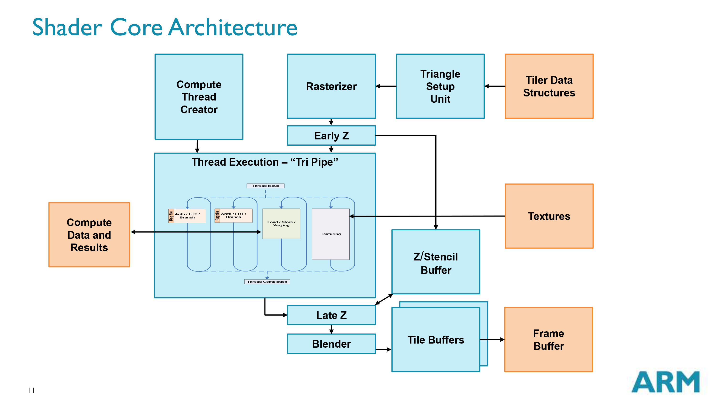
Another interesting point to make about the Mali architecture (that goes unnoticed, but is significant) is that the anti-aliasing is fully pipelined, tiled (read zero bandwidth penalty for the op), and very fast. MSAA 4x costs 1 cycle, MSAA 8x costs 2 cycles, and MSAA 16x costs 4 cycles. This means that if you have a scene full of fragment shaders running for more than 4 cycles (which is not too complex these days) you get the benefit of ultra-high quality MSAA 16x for FREE.There aren't too many examples of MSAA 16x online, but even at MSAA 8x performs very well, with sharp, non-blurry results and is often compared against. MSAA would produce very crisp edges devoid of aliasing and crawling during animation.
Of course, MSAA isn't perfect -- it isn't terribly helpful for deferred renderers -- but it certainly doesn't hurt them when its costs are nothing, even if you are planning to do a screen-space pass in post.
toyotabedzrock - Friday, July 4, 2014 - link
Oddly the best open source driver is for adreno GPU, perhaps you should ask that person what he knows about it?ol1bit - Saturday, July 5, 2014 - link
This is another fantastic job guys! Thanks to you and Thanks to Midgard for sharing!cwabbott - Saturday, July 5, 2014 - link
Well, if they won't cough up the information, then there's always freedreno... Rob Clark has reverse engineered basically everything you would want to know about the Adreno architecture, up to even more detail than this article. All that remains is to fill in the pieces based on the documentation he's written...