ARM’s Mali Midgard Architecture Explored
by Ryan Smith on July 3, 2014 11:00 AM ESTMidgard’s Arithmetic Pipelines
Having taken a look at Midgard’s architecture from a high level perspective, we next want to dive deep into the heart of Midgard: its arithmetic pipelines. This is where the bulk of the work takes place on any modern GPU, and in most cases real-world GPU performance significantly hinges on the design decisions made here. Furthermore this is where Midgard’s most unconventional design decisions lie, and as a result it’s the arithmetic pipelines that make Midgard stand apart from anything else we’ve seen.
ARM describes Midgard as a Very Long Instruction Word (VLIW) design with Single Instruction Multiple Data (SIMD) characteristics (though officially it is called Sequential Long Instruction Word). What this means is that at a high level ARM is feeding multiple ALUs, including SIMD units, with a single long word of instructions. But perhaps it’s better we start at a low level instead.
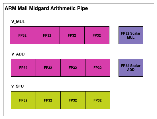
The above is a single Midgard arithmetic pipeline, in our example configured for FP32 operations. In it ARM uses a mix of both scalar and vector (SIMD) ALUs. Altogether ARM breaks it down as 3 vector ALUs and 2 scalar ALUs, each responsible for a specific type of operation.
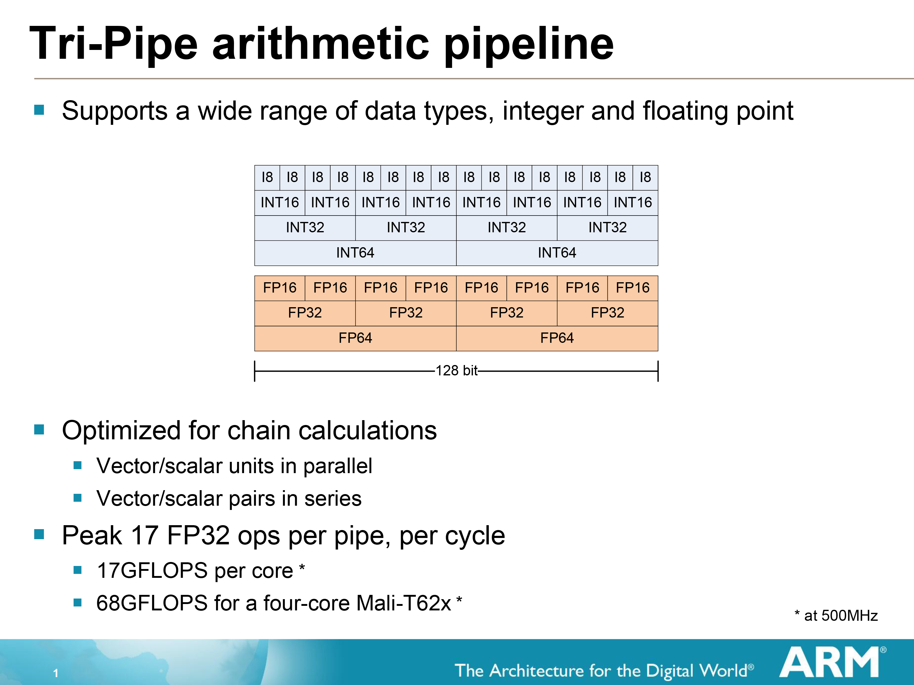
If we stop for a moment and look at the SIMD, we find out something very interesting about it as well. Remember earlier how we mentioned that Midgard is capable of 64bit operations? Well this is how they do it. Not with separate 64bit and 32bit units as in some other designs, but by using a single 128bit wide SIMD and decomposing operations based on their width. The 128bit SIMDs in a Midgard core can process 2 64 bit operations, 4 32bit operations, or even 8 16bit operations per clock cycle. Simply fill the SIMD with as many (identical) operations as will fit, and the SIMD will handle the rest.
The use of SIMDs and SIMD-like designs is not uncommon in GPUs, but it’s relatively rare to see a flexible SIMD of this nature. In the past other architecture designers have talked about this being a efficiency tradeoff – you lose some efficiency by using a flexible design rather than a rigid design – however in ARM’s case they have decided that they can meet all of their goals with a 128bit SIMD.
Jumping back up a level, from a hardware perspective a Midgard arithmetic pipeline is capable of up to 17 FP32 FLOPS. This is constructed as the following.
- 4 vector adds
- 4 vector multiplies
- 1 scalar add
- 1 scalar multiple
- 1 FDOT4 dot product (7 FLOPS)
The vector and scalar operations are relatively self-explanatory, while the dot products are a result of using the vector special functions unit. To that end every architecture possesses SFUs in some form to handle dot products, transcendentals, and other complex operations, but their inclusion in FLOPS counting is uncommon. Most architectures merely count FLOPS as adds and multiplies through the ubiquitous and all important MAD (Multiply-Add) instruction. NVIDIA’s forthcoming K1 (to pick a GPU with a desktop counterpart) has 192 FP32 ALUs, and via MADs can achieve up to 384 FLOPS per cycle.
Ultimately how ARM counts FLOPS is entirely up to them, but we do want to take a moment to rectify it with how we count FLOPS on our end. Dot products are a relatively common mathematical operation in rendering, enough so that it’s important to be able to do them quickly, but they are generally not counted for computing FLOPS.
Meanwhile for FP64 FLOPS, as one would expect Midgard’s performance is much lower. ARM does not provide the FLOPS breakdown for 64bit operations, but they tell us that it is a total of 5 FLOPS. Our best guess here is that 4 of those FLOPS are coming from the vector units (2 FP64 MADs) and then 1 more FP64 FLOP is coming off of the scalar units, which if our assumption is correct would imply that it is not capable of an FP64 MAD in 1 cycle. Overall on a MAD basis this puts FP64 performance at 5/10ths, or ½ FP32 performance, which is a very high FP64 performance ratio even compared to desktop GPU architectures.
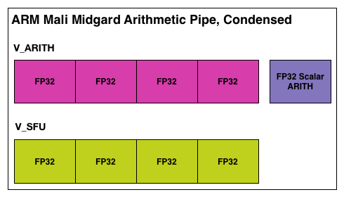
Furthermore, in further rectifying how ARM presents some of its data with how we typically present data in our articles, we’re also going to be using a condensed version of the Midgard arithmetic pipeline from this point on. As most architectures either utilize ALUs that can perform a MAD on their own or simplify their descriptions to showcase 1 ALU (rather than explicitly over 2 ALUs as on Midgard), we will be using a condensed version of the Midgard arithmetic pipeline that is drawn in a similar manner. Since we always count a standard ALU as being capable of 2 FLOPs (SFUs withstanding), this makes our Midgard arithmetic pipeline illustration consistent with our previous illustrations. It’s for all intents and purposes the same pipeline, only condensed.
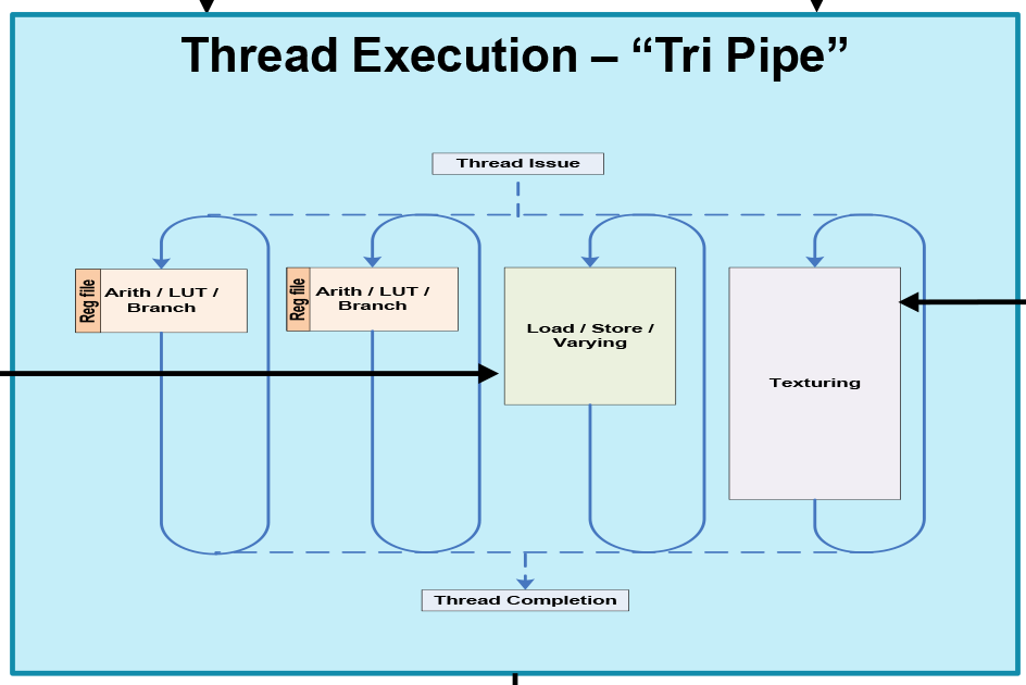
Finally, let’s take a quick look at a complete Midgard “tri pipe” core from an ALU standpoint. Since in T760 each core has 2 arithmetic units, a single core a just 2 of our condensed units. For a complete GPU this would then be multiplied by as many cores as the resulting design called for.


66 Comments
View All Comments
kkb - Monday, July 7, 2014 - link
I hope you do understand how to read benchmark results. 3dmark and GFXbench(offscreen) results are resolution independent. Now go and check the results in the article.As per T760, I will not comment on theoretical GFLOP numbers unless there is real product. Even the theoretical MAD GFLOPs are not so great (roughly half) compared to others. I don't think anyone going to fall for marketing gimmick of taking dot product also as extra 40 GFLOPs
darkich - Monday, July 7, 2014 - link
You said it definitely performs better yet it loses on the T Rex HD onscreen and in Basemark X overall. That's not definite you know.Regardless, even if a case can be made that it performs slightly better overall than the Mali T628, it is without doubt outperformed by the :
ULP Gforce 3
Adreno 330
Sgx G6320
.. and is *definitely* far outclassed by the Adreno 420, Kepler K1, SGX G6550, Mali T760MP6-10.
Until Intel shows their next generation of ULP graphics, I don't see a point in comparing the current one
darkich - Monday, July 7, 2014 - link
Correction, I believe the GPU in Tegra 4 is internally referred to as the ULP GeForce 4, not 3fithisux - Friday, July 4, 2014 - link
Could you provide an expository of C66x architecture since it is suitable in my opininion for GPGPU tasks and realtime software rendering/raytracingjann5s - Friday, July 4, 2014 - link
lol, I thought this expression was wrong: "the proof is in the pudding", but in fact I was wrong: http://en.wiktionary.org/wiki/the_proof_is_in_the_...toyotabedzrock - Friday, July 4, 2014 - link
I wish you would have talked more about the GPU in the Nexus 10 since that is a shipping product. It would be nice to know how it differs from the newer midgard designs.seanlumly - Friday, July 4, 2014 - link
Another interesting point to make about the Mali architecture (that goes unnoticed, but is significant) is that the anti-aliasing is fully pipelined, tiled (read zero bandwidth penalty for the op), and very fast. MSAA 4x costs 1 cycle, MSAA 8x costs 2 cycles, and MSAA 16x costs 4 cycles. This means that if you have a scene full of fragment shaders running for more than 4 cycles (which is not too complex these days) you get the benefit of ultra-high quality MSAA 16x for FREE.There aren't too many examples of MSAA 16x online, but even at MSAA 8x performs very well, with sharp, non-blurry results and is often compared against. MSAA would produce very crisp edges devoid of aliasing and crawling during animation.
Of course, MSAA isn't perfect -- it isn't terribly helpful for deferred renderers -- but it certainly doesn't hurt them when its costs are nothing, even if you are planning to do a screen-space pass in post.
toyotabedzrock - Friday, July 4, 2014 - link
Oddly the best open source driver is for adreno GPU, perhaps you should ask that person what he knows about it?ol1bit - Saturday, July 5, 2014 - link
This is another fantastic job guys! Thanks to you and Thanks to Midgard for sharing!cwabbott - Saturday, July 5, 2014 - link
Well, if they won't cough up the information, then there's always freedreno... Rob Clark has reverse engineered basically everything you would want to know about the Adreno architecture, up to even more detail than this article. All that remains is to fill in the pieces based on the documentation he's written...