NVIDIA Tegra 4 Architecture Deep Dive, Plus Tegra 4i, Icera i500 & Phoenix Hands On
by Anand Lal Shimpi & Brian Klug on February 24, 2013 3:00 PM ESTNVIDIA has upped its ISP game with Tegra 4, and includes the same ISP in both Tegra 4 and 4i, which they’ve dubbed Chimera. This new ISP includes a number of features which were already demonstrated at CES, but NVIDIA went into greater detail.

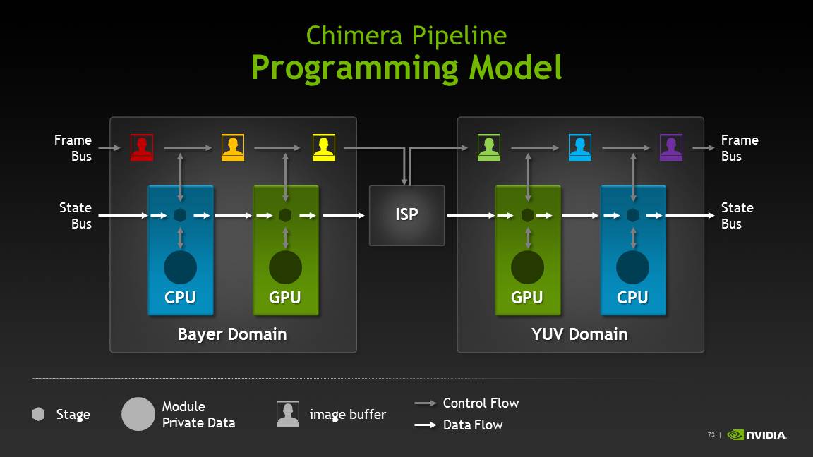
NVIDIA’s major new feature with Tegra 4 is inclusion of new APIs which leverage the GPU to enable computational camera features In addition to the traditional ISP pipeline. To begin, NVIDIA has made their own enhancements in the imaging chain which leverage this GPU-assisted architecture that sits atop the normal ISP. They’ve outlined a few features which work atop this — HDR panorama, HDR stills, and real time object tracking. The end result is that Chimera is one part programming model and APIs for future development efforts by third parties, another part first party software that NVIDIA will distribute for integration in OEM cameras which includes the HDR features and object tracking.
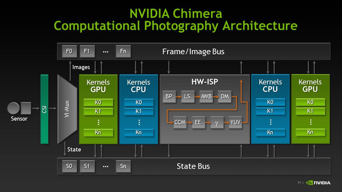
Chimera allows developers to build blocks around the traditional ISP data flow and get to manipulate either bayer image data or YUV space image data on the CPU or GPU using their own framework. There are still a lot of details to come about the programming model and how this will be exploited, but there clearly is space here for NVIDIA to try and make a case for their GPU being useful for image processing. At the same time, the elephant in the room is OpenCL (and its current absence on Tegra 4) and what direction the industry will take that to leverage GPU compute for some computational photography processing.
The novel new feature of note is something I was skeptical about upon seeing at CES — single frame HDR video. The traditional route for HDR video capture is to capture at twice the framerate of the intended output video, for example for 720p30 video with a two-frame HDR, that would mean capture at 720p60 with two different exposures. What NVIDIA does is a bit different. Instead of capturing two exposures and combining them after capture, NVIDIA has found a way to drive selected CMOS sensors (both IMX135 from Sony and AR0833 from Aptina have been called out specifically, but there are more) in some special fashion, and recombine interleaved high and low exposure images (the +1 stop, –1 stop) image into one equivalent frame. This is all done on the GPU using the same Chimera pipeline blocks, but with NVIDIA’s own algorithm. The results are actually pretty impressive, NVIDIA claims 3 stops of dynamic range (~24 dB), and no recombination artifacts.
Previous demonstrations of HDR video capture on a few other platform have had halos around moving elements because of the issues associated with taking two temporally different frames and recombining them. With NVIDIA’s HDR video capture I saw no halos even on very fast moving objects, with the same quality of HDR.
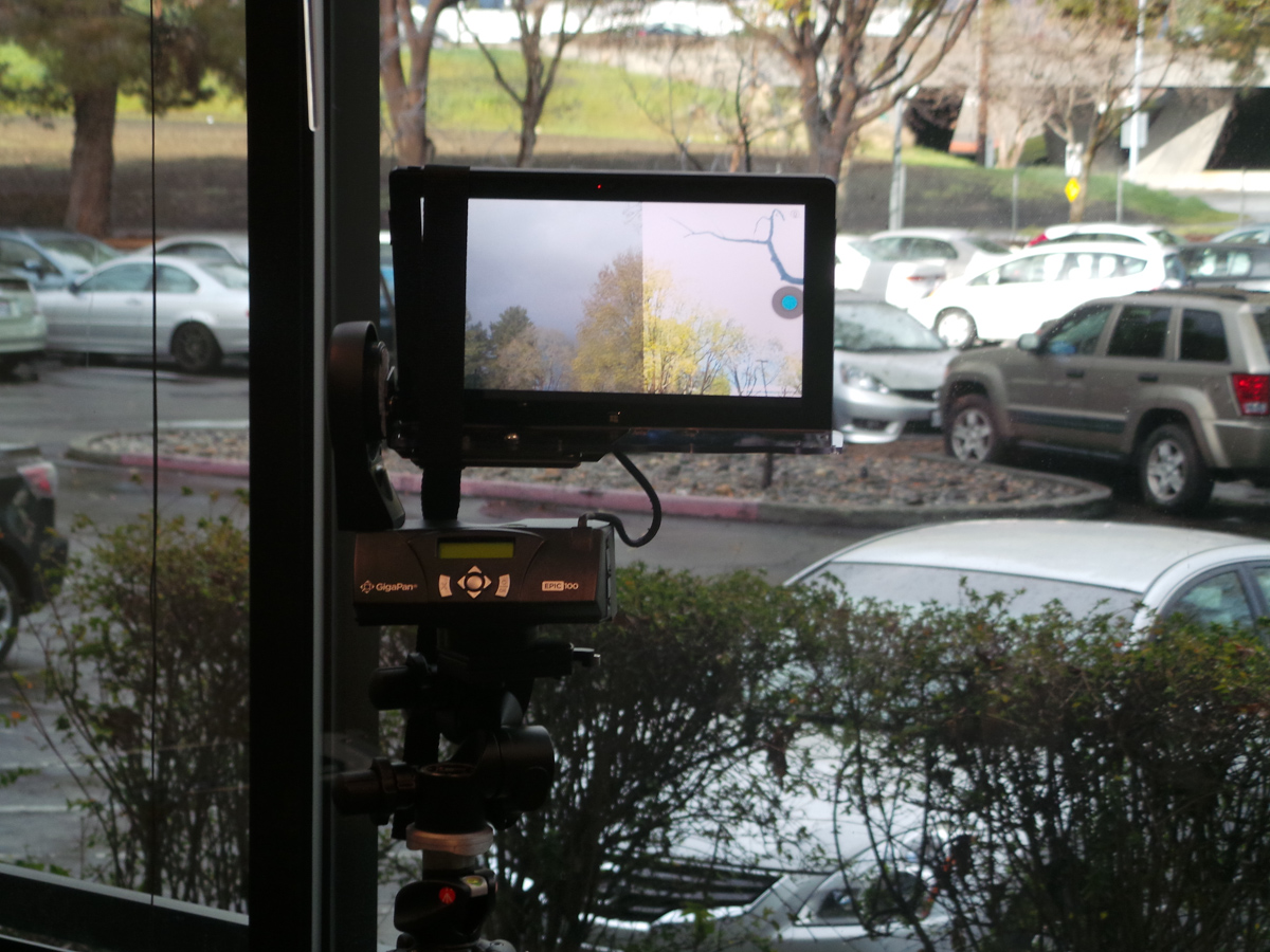
NVIDIA also demonstrated their panorama capture which includes HDR as well, using a GigaPan Epic 100. Admittedly a better demo might be hand held to demonstrate how well the ISP is able to compensate for change in perspective from the tablet moving around in the hand, the resulting image was the same quality of HDR as the still however. I also saw object tracking which essentially is face tracking (and thus AE / AF assist to that subject) but taken to arbitrary subjects. Paint a box around the object you want to track, and the camera will perform feature extraction and machine learn a model around the object. Rotating around complex geometries seemed to work decently well — the model learns slowly so slow movements can be accommodated, faster moving subjects might not be object tracked.

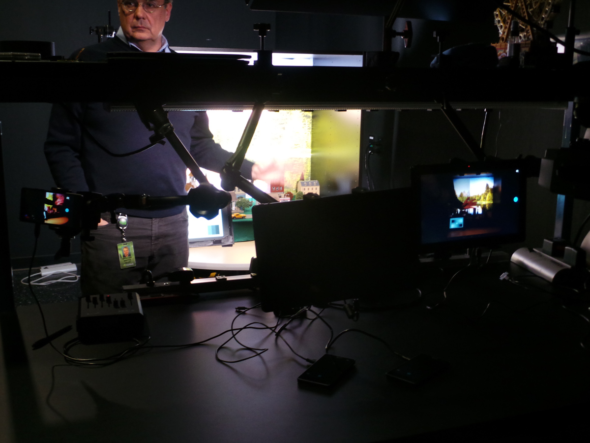
I also got a chance to tour NVIDIA’s camera tuning labs, where they characterize smartphone CMOSes for handset markers, and work with them on tuning their ISP and imaging experience. I saw one calibration room with many different scenes, and then another room with large test charts, and two sets of standard test scenes in lightboxes. The ever-familiar GMB color checker card and ISO12233 charts were everywhere as well.


75 Comments
View All Comments
Krysto - Monday, February 25, 2013 - link
S600 is just a slightly overclocked S4 Pro with the same GPU.The real competitor of Tegra 4 will be S800. We'll see if it wins in CPU performance (it might not), and I think there's a high chance it will lose in GPU performance, as Adreno 330 is only 50% faster than Adreno 320 I think, and Tegra 4 is about twice as fast.
Qualcomm has always had slower graphics performance than Nvidia actually. The only "gap" they found in the market was last fall with the Adreno 320, when Nvidia didn't have anything good to show. But Tegra 3 beat S4 with its Adreno 225.
watersb - Monday, February 25, 2013 - link
I'm amazed at the depth of this NVIDIA data-dump. Brilliant work.Anand's observation re: die size, cost strategy, position in the market and how this buys them time to consolidate... Wow.
Clearly, Nvidia is in this game for the long haul.
djgandy - Monday, February 25, 2013 - link
So OpenGL ES 3.0 doesn't matter, but quad core A15 does? Why do people suck up to Nvidia and their marketing BS so much?T4i still single channel memory? What a joke configuration.
djgandy - Monday, February 25, 2013 - link
Also a 9 page article about a mobile SoC without a single reference to the word "battery".varad - Monday, February 25, 2013 - link
Read the article before you write such comments. The very first page is "Introduction & Power" where they do mention some numbers and their thoughts.djgandy - Tuesday, February 26, 2013 - link
Yeah its all smoke and mirrors under lab test conditions. Where is the real battery life? Is this not for battery powered devices?Krysto - Monday, February 25, 2013 - link
Personally, I think all 2013 GPU's should have support for OpenGL ES 3.0 and OpenCL. I was stunned to find out Tegra 4 was not going to support it as they haven't even switched to a unified shader architecture.That being said, Anand is probably right that it was the right move for Nvidia, and they are just going to wait for the Maxwell architecture to streamline the same custom ARMv8 CPU from Tegra 5 to Project Denver across product line-ups, and also the same Maxwell GPU cores.
If that's indeed their plan, then switching Tegra 4 to Kepler this year, only to switch again to Maxwell next year wouldn't have made any sense. GPU architectures barely change even every 2-3 years, let alone 1 year. It wouldn't have been cost effective for them.
I do hope they aren't going to delay the transition again with Tegra 5 though, and I also do hope they follow Qualcomm's strategy with S4 last year of switching IMEMDIATELY to the 20nm process, instead of continuing on 28nm with Tegra 5, like they did with Tegra 3 on 40nm. But I fear Nvidia will repeat the same mistake.
If they put Tegra 5 on 20nm, and make it 120mm2 in size, with Maxwell GPU core, I don't think even Apple's A8X will stand against it next year in terms of GPU performance (and of course it will get beaten easily in CPU performance, just like this year).
djgandy - Tuesday, February 26, 2013 - link
Tegra is smaller because it lacks features and also memory bandwidth. The comparison is not really fair to assume you can just throw more shaders at the problem. You'll need wider memory bus for a start. You'll need more TMU's and in the future it's probably smart to have a dedicate ROP unit. Then also are you seriously going to just stick with FP20 and not support ES 3.0 and OpenCL? OEMs see OpenCL as a de facto feature these days, not because it is widely used but because it opens up future possibilities. Nvidia has simply designed an SoC for gaming here.Your post focuses on performance, but these are battery powered devices. The primary design goal is efficiency, and it would appear that is why apple went swift and not A15. A15 is just too damn power hungry, even for a tablet.
metafor - Tuesday, February 26, 2013 - link
If the silicon division of Apple were its own business, they'd be in the red. Very few silicon providers can afford to make 120mm^2 chips and still make a profit; let alone one with as little bargaining clout in the mobile space as nVidia.Numbers are great but at the end of the day, making money is what matters.
milli - Monday, February 25, 2013 - link
nVidia is trying hard but Tegra still isn't making them any money ...