AMD Radeon HD 7970 Review: 28nm And Graphics Core Next, Together As One
by Ryan Smith on December 22, 2011 12:00 AM EST- Posted in
- GPUs
- AMD
- Radeon
- ATI
- Radeon HD 7000
Theoreticals & Tessellation
From a rendering perspective one of the most interesting things AMD did with Tahiti was what they didn’t do: they didn’t add more ROPs, they didn’t add more geometry engines. And yet based on our game performance they’ve clearly improved on their performance in those situations by making more efficient use of the hardware they do have.
So we wanted to take a quick look at synthetic performance to see what these tools had to say about AMD’s changes. We’ve included the numbers for every other GPU in our lineup as a reference point, but we would strongly suggest against reading into them too much. AMD versus AMD is sometimes relevant to real world performance; AMD versus NVIDIA rarely is.
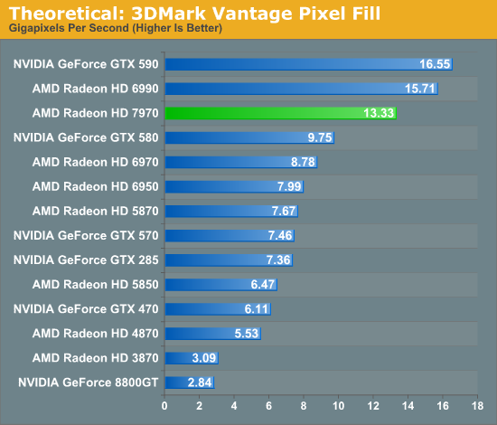
We’ll start with 3DMark Vantage and its color fill test. This is basically a ROP test that attempts to have a GPU’s ROPs blend as many pixels as it can. Theoretically AMD can do 32 color operations per clock on Tahiti, which at 925MHz for 7970 means the theoretical limit is 29.6Gpix/sec; not that any architecture is ever that efficient. In practice 7970 hits 13.33Gpix/sec, which is still well short of the theoretical maximum, but pay close attention to 7970’s performance relative to 6970. Even with the same number of ROPs and a similar theoretical performance limit (29.6 vs 28.16), 7970 is pushing 51% more pixels than 6970 is.
In designing Tahiti AMD said that they didn’t need more ROPs they just needed more efficient ROPs, and it looks like they’ve delivered on this. It’s not clear whether this is the limit for efficiency or if AMD can squeeze more out of their ROPs in future designs, but this definitely helps to prove that there’s more to graphics rendering than a large number of functional units.
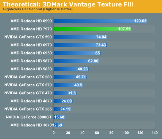
Our other 3DMark synthetic benchmark is the 3DMark Vantage Texture Blend test, which measures how quickly a GPU can blend multiple FP16 textures. This is more synthetic than most tests because FP16 textures aren’t widely used, but it’s a consistent benchmark.
The theoretical performance improvement from 6970 to 7970 is 40% - 33% more texture units operating at a 5% higher clockspeed. In practice the 7970 exceeds that improvement by increasing texture performance by 46%, meaning the 7970 has benefitted from more than the increase in texture units. Most likely the new cache architecture has further improved the efficiency of the texture units, although the 3DMark texture set is not particularly large.
Moving on, we also wanted to take a look at tessellation. AMD did not increase the theoretical geometry performance of Tahiti as compared to Cayman – both top out at 2 triangles per clock – but AMD has put a lot of effort into improving the efficiency of Tahiti’s geometry units as we’ve seen reflected in our game benchmarks.
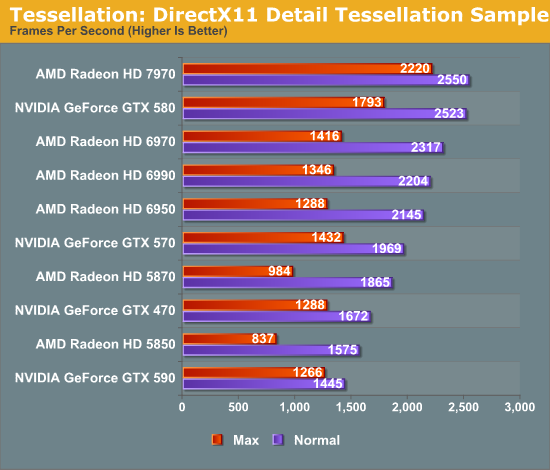
Our first tessellation benchmark is the traditional Detail Tessellation sample program from the DirectX SDK. Here we’re looking at tessellation performance as a product of the framerate, testing at tessellation factors 7 (normal) and 15 (max). Traditionally this is a test that has been rather balanced at normal tessellation levels, while NVIDIA cards with their superior geometry throughput have been the top performers at maximum tessellation levels. So it’s all the more interesting when we’ve seen the tables turned; the 7970 is merely competitive with the GTX 580 at normal tessellation levels, but now it’s ahead of the GTX 580 by 24%. More significantly however the 7970 is ahead of the 6970 by 57%.
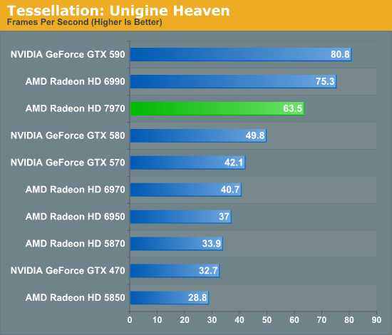
Our second tessellation benchmark is Unigine Heaven, a benchmark that straddles the line between a synthetic benchmark and a real-world benchmark, as the engine is licensed but no notable DX11 games have been produced using it yet. In any case the Heaven benchmark is notable for its heavy use of tessellation, which means it’s largely a proxy test for tessellation performance.
As with the Detail Tessellation sample program, Heaven shows significant gains for the 7970 versus the 6970, with the 7970 leading by 56%. Meanwhile it leads the GTX 580 by 27%, which is actually slightly better than what we saw under the more “pure” Detail Tessellation sample. Between these two benchmarks it’s clear that AMD’s tessellation efficiency improvements are quite real, and that with Tahiti AMD can deliver much better tessellation performance than Cayman even at virtually the same theoretical triangle throughput rate.
Of course one has to wonder what NVIDIA will have in store for Kepler next year. Their current Fermi design seems to scale well with additional geometry units, but if Tahiti is anything to go by, there’s a great deal to be gained just by focusing on efficiency. NVIDIA has prided themselves on their geometry performance since before GF100 even shipped, so it will be interesting if they have anything in store to hold on to that distinction.


292 Comments
View All Comments
Zingam - Thursday, December 22, 2011 - link
And at the time when it is available in D3D. AMD's implementation won't be compatible... :D That's sounds familiar. So will have to wait for another generation to get the things right.Ryan Smith - Thursday, December 22, 2011 - link
As for your question about FP64, it's worth noting that of the FP64 rates AMD listed for GCN, "0" was not explicitly an option. It's quite possible that anything using GCN will have at a minimum 1/16th FP64.Sind - Thursday, December 22, 2011 - link
Excellent review thanks Ryan. Looking forward to see what the 7950 performance and pricing will end up. Also to see what nv has up their sleeves. Although I can't shake the feeling amd is holding back.chizow - Thursday, December 22, 2011 - link
Another great article, I really enjoyed all the state-of-the-industry commentary more than the actual benchmarks and performance numbers.One thing I may have missed was any coverage at all of GCN. Usually you guys have all those block diagrams and arrows explaining the changes in architecture. I know you or Anand did a write-up on GCN awhile ago, but I may have missed the link to it in this article. Or maybe put a quick recap in there with a link to the full write-up.
But with GCN, I guess we can close the book on AMD's past Vec5/VLIW4 archs as compute failures? For years ATI/AMD and their supporters have insisted it was the better compute architecture, and now we're on the 3rd major arch change since unified shaders, while Nvidia has remained remarkably consistent with their simple SP approach. I think the most striking aspect of this consistency is that you can run any CUDA or GPU accelerated apps on GPUs as old as G80, while you even noted you can't even run some of the most popular compute apps on 7970 because of arch-specific customizations.
I also really enjoyed the ISV and driver/support commentary. It sounds like AMD is finally serious about "getting in the game" or whatever they're branding it nowadays, but I have seen them ramp up their efforts with their logo program. I think one important thing for them to focus on is to get into more *quality* games rather than just focusing on getting their logo program into more games. Still, as long as both Nvidia and AMD are working to further the compatibility of their cards without pushing too many vendor-specific features, I think that's a win overall for gamers.
A few other minor things:
1) I believe Nvidia will soon be countering MLAA with a driver-enabled version of their FXAA. While FXAA is available to both AMD and Nvidia if implemented in-game, providing it driver-side will be a pretty big win for Nvidia given how much better performance and quality it offers over AMD's MLAA.
2) When referring to active DP adapter, shouldn't it be DL-DVI? In your blurb it said SL-DVI. Its interesting they went this route with the outputs, but providing the active adapter was definitely a smart move. Also, is there any reason GPU mfgs don't just add additional TMDS transmitters to overcome the 4x limitation? Or is it just a cost issue?
3) The HDMI discussion is a bit fuzzy. HDMI 1.4b specs were just finalized, but haven't been released. Any idea whether or not SI or Kepler will support 1.4b? Biggest concern here is for 120Hz 1080p 3D support.
Again, thoroughly enjoyed reading the article, great job as usual!
Ryan Smith - Thursday, December 22, 2011 - link
Thanks for the kind words.Quick answers:
2) No, it's an active SL-DVI adapter. DL-DVI adapters exist, but are much more expensive and more cumbersome to use because they require an additional power source (usually USB).
As for why you don't see video cards that support more than 2 TMDS-type displays, it's both an engineering and a cost issue. On the engineering side each TMDS source (and thus each supported TMDS display) requires its own clock generator, whereas DisplayPort only requires 1 common clock generator. On the cost side those clock generators cost money to implement, but using TMDS also requires paying royalties to Silicon Image. The royalty is on the order of cents, but AMD and NVIDIA would still rather not pay it.
3) SI will support 1080P 120Hz frame packed S3D.
ericore - Thursday, December 22, 2011 - link
Core Next: It appears AMD is playing catchup to Nvidia's Cuda, but to an extent that halves the potential performance metrics; I see no other reason why they could not have achieved at varying 25-50% improvement in FPS. That is going to cost them, not just for marginally better performance 5-25%, but they are price matching GTX 580 which means less sales though I suppose people who buy 500$ + GPUs buy them no matter what. Though in this case, they may wait to see what Nvidia has to offer.Other New AMD GPUs: Will be releasing in February and April are based on the current architecture, but with two critical differences; smaller node + low power based silicon VS the norm performance based silicon. We will see very similar performance metrics, but the table completely flips around: we will see them, cheaper, much more power efficient and therefore very quiet GPUs; I am excited though I would hate to buy this and see Nvidia deliver where AMD failed.
Thanks Anand, always a pleasure reading your articles.
Angrybird - Thursday, December 22, 2011 - link
any hint on 7950? this card should go head to head with gtx580 when it release. good job for AMD, great review for Ryan!ericore - Thursday, December 22, 2011 - link
I should add with over 4 billion transistors, they've added more than 35% more transistors but only squeeze 5-25% improvement; unacceptable. That is a complete fail in that context relative to advancement in gaming. Too much catchup with Nvidia.Finally - Thursday, December 22, 2011 - link
...that saying? It goes like this:If you don't show up for a race, you lose by default.
Your favourite company lost, so their fanboys may become green of envydia :)
Besides that - I'd never shell out more than 150€ for a petty GPU, so neither company's product would have appealed to me...
piroroadkill - Thursday, December 22, 2011 - link
Wait, catchup? In my eyes, they were already winning. 6950 with dual BIOS, unlock it to 6970.. unbelievable value.. profit??Already has a larger framebuffer than the GTX580, so...