Analyzing Falkor’s Microarchitecture: A Deep Dive into Qualcomm’s Centriq 2400 for Windows Server and Linux
by Ian Cutress on August 20, 2017 11:00 AM EST- Posted in
- CPUs
- Qualcomm
- Enterprise
- SoCs
- Enterprise CPUs
- ARMv8
- Centriq
- Centriq 2400
The Duplex and Power Management
Like many processors on the market, design companies will use building blocks to assemble their complete processors. Equip those blocks with the right protocols, put them together, optimize, and create an advanced piece of sand that can decompress cat gifs if we prod it in the right way. Qualcomm’s main building block at the SoC level is the Falkor duplex, containing two Falkor cores, a shared L2 cache, QSB/fabric connectivity, and represents the lowest level of power management.
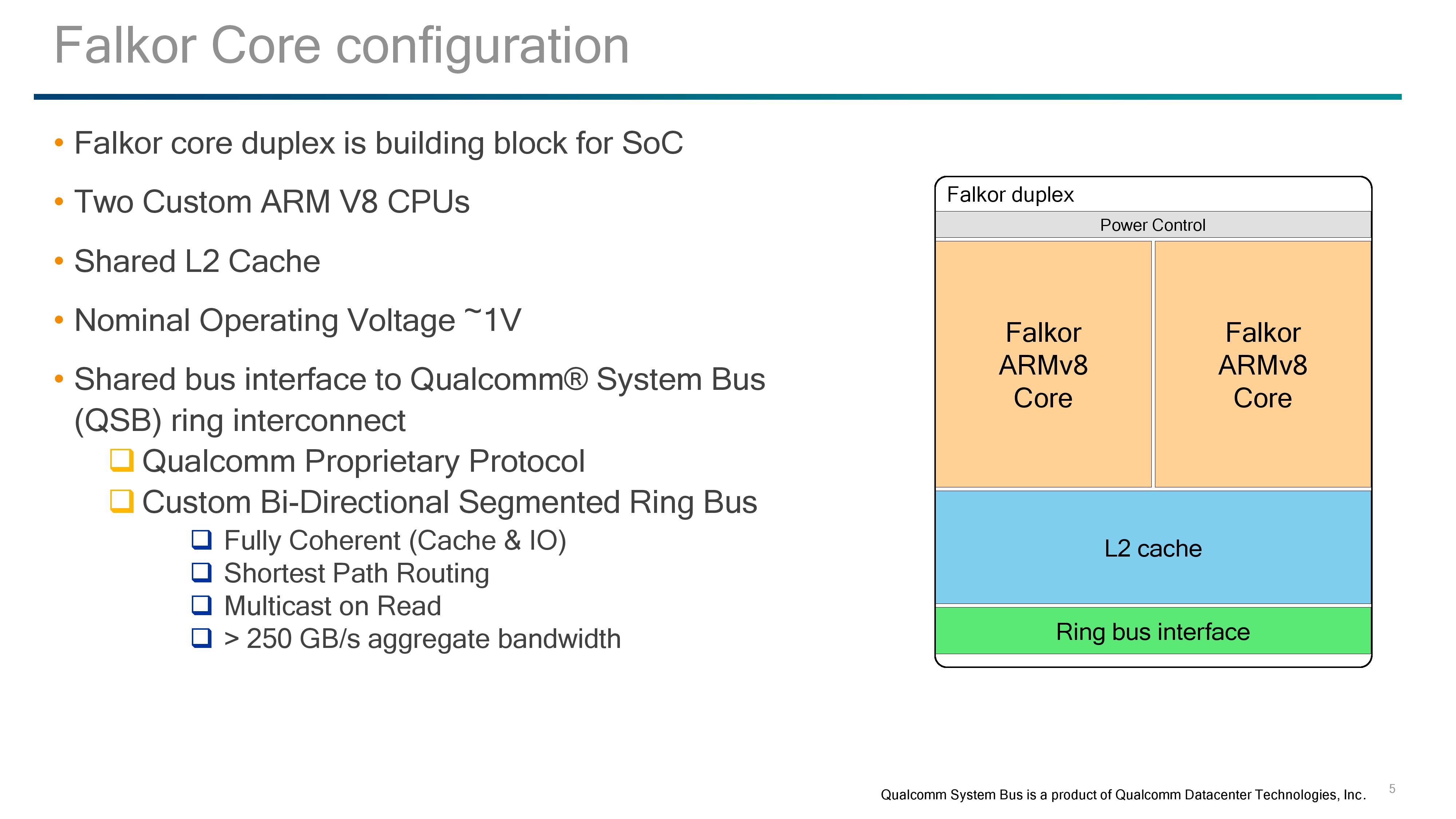
For SoC design followers, one might look at this design and think they see similarities with other dual-core designs such as AMD’s original Bulldozer design from 2011 or Intel's Xeon Phi. Internally, the cores are completely separate in terms of instruction throughput with no shared resources before the L2 cache. Consequently, between the two ends of the spectrum, Falkor is much closer to a Xeon Phi dual-core module, where each core has its own set of execution ports and vector extensions, but share an L2 cache and network connectivity.
But before diving into the cores, the L2 cache and power control require some explaining.
The L2 cache is a unified cache between both cores with ECC support, and inclusive of the L1-Data caches on both. Accesses are 128-byte interleaved with 128-byte lines, with 32-bytes per direction per interleave per cycle and 8-way associativity. ECC is using SEC-DED methodology, and the overall result as a minimum 15 cycle latency for an L2 hit, which is very competitive in the market. Qualcomm isn’t stating the size of the L2 cache at this time, which is somewhat of a surprise. In the market we see a variety of L2 cache options, so Qualcomm might end up offering a series of processors with different amounts of L2, especially if L2 defects are a factor in the manufacturing.

For power control, Qualcomm uses this unified design to control both cores. During our briefing we were told that both cores have to share the same frequency for L2 consistency; however the voltage per core can be adjusted and optimized for the best power implementation. As a result, power states between the cores can vary, and depending on the workflow needed, the cores and the L2 can also have different power states.
The cores in the duplex are powered by a block head switch or a low-dropout regulator (LDO), depending on the requirement. This allows for a variety of power down modes for the core logic, registers and caches:
- Light Sleep: CPU Clock is gated/lowered
- Voltage Retention: Registers and Caches retain state, logic is effectively off
- Register Retention: Registers retail state using main chip power rail, caches are off
- Collapse: Registers and L1 state not retained
The power control also maintains the state of the L2 cache, which offers modes similar to the CPU and may clock gate completely even with the CPUs in use. We confirmed that the L2 cache can only be on or off, and not in a half-use state.
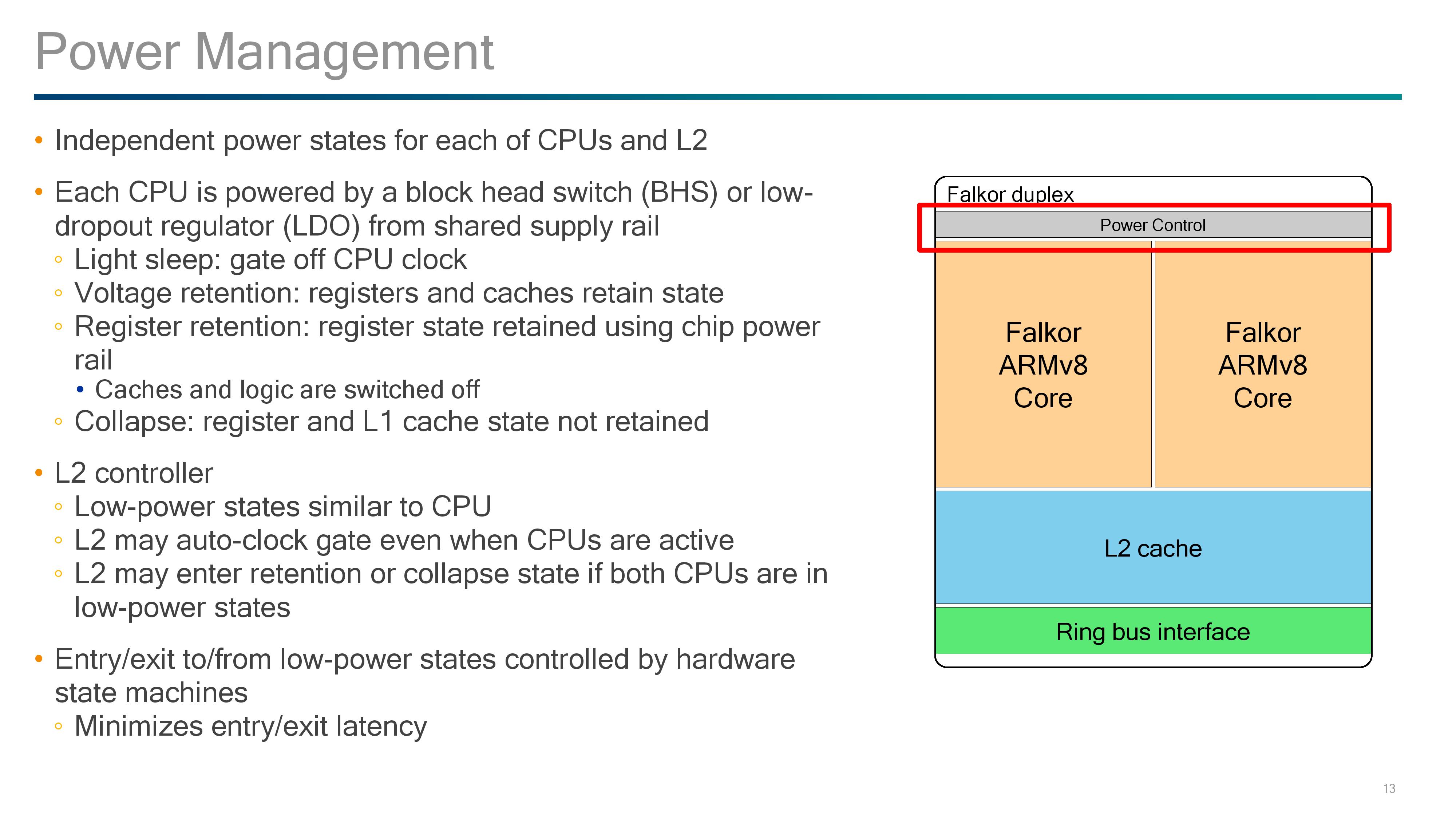
Overall for power, Qualcomm is also implementing hardware state machines, to enable quick entry and exit to and from low power modes. Qualcomm explained that CPU use in data centers can be super low depending on time of day and requirements, so the ability to save power wake quickly was a fundamental design aspect for this chip, with the aim of reducing the electricity bill.
We know that these chips are built on a 10nm process, and when questioned Qualcomm stated that they will run above 2.0 GHz, while talking in about 1.0 V to do so while also being competitive in performance per watt. Unfortunately requests regarding TDP were returned with 'competitive for a data center environment'.


41 Comments
View All Comments
DanNeely - Sunday, August 20, 2017 - link
Mobile CSS needs fixed. Bulleted lists need to wrap, instead of overflowing into horizontal scroll as they currently do on Android.twotwotwo - Sunday, August 20, 2017 - link
The things I most wonder about the chip itself are, how much worse will single-thread speed be, and how much better will throughput/$ be?For serial speed, there's sort of a sliding scale of "good enough"; you can certainly find uses for chips that are slower than Intel's large cores, but as single-thread perf gets worse and worse, more types of app become tricky to run on it because of latency. So you want latency stats for typical enterprisey Java or C# (or, heck, Go) Web app or widely used databases or infrastructure tools. That's also a test of how well compilers and runtimes are tuned for ARMV8, the chip, and live with may cores, but since early customers will have to deal with the ecosystem that exists today, that's reasonable.
For cost-effective throughput I guess we need to have an idea of at least price and power consumption, and parallel benchmarks that will hit bottlenecks a single-threaded one might not, like memory bandwidth. And the toughest comparison is probably against Intel's parts in the same segment, Xeon D and their server Atom chips. Something that makes it harder to win big on throughput/$ is that the CPU's cost and power consumption are only a piece of the total: DRAM, storage, network, and so on account for a lot of it. Also, the big cloud customers Qualcomm wants to win probably aren't paying the same premiums as you and I are to Intel.
Then, aside from questions about the chip itself, there are questions about the ecosystem and customers. There are the questions above of how well toolchains and software are tuned. Maybe the biggest question is whether some big customer will make the leap and do some deployments on lots of slower cores. It might be a strategic long-term bet for some big cloud company that wants more competition in the server chip space, but I bet they have to be willing to lose real money on the effort for a generation or two first.
name99 - Monday, August 21, 2017 - link
Intel sells 28 core CPUs that run at 2.1 GHz (and turbo up to 3.8GHz but see below).Hell, they sell 16 core systems that run at 2.0 GHz and only turbo up to 2.8 GHz.
Remember QC is not TRYING to sell these to amateurs, or even as office servers. They are targeted at data warehouse tasks where the job they're doing will be pretty well defined, and it's expected for the most part that ALL the cores will be running (ie when the work load lightens, you shut down entire dies and then racks, you don't futz around with just shutting down single cores).
For environments like that, turbo'ing is of much less value. QC doesn't have to (and isn't) targeting the entire space of HPC+server+data warehouse, just the part that's a good match to what they're offering.
Threska - Tuesday, August 22, 2017 - link
Well there is the small developer virtualization market like Ansible.prisonerX - Monday, August 21, 2017 - link
A preoccupation with single thread performance is the domain of video game playing teenagers and not terribly important, neither is the "latency" you refer to. This sort of high-core, efficient processor is going to be used where throughput and price/power/performance ratio (ie, all three, not just any one of those), are the key metric.Latency is mostly irrelevant since processing will be stream oriented and bandwidth limited rather than hamstrung by latency (thus features such as memory bandwidth compression). Gimmicks like "turbo" (which should be called by its proper name: "throttling") and favoring single thread performance are counterproductive in this mode. Being able to deploy many CPUs in dense compute nodes is what is required and memory, storage and networking are minor parts here.
I don't know why you think compilers or runtimes is a concern, 99.9% of code is common across archs, so if you've supported a lot of x86 cores your code is going to function well for a lot of ARM cores with a small amount of arch specific configuration. The compilers themselves, namely GCC and LLVM are mature as is their support for ARM.
Finally the new ARM CPUs don't have to beat Intel, just stay roughly competitive, because the one thing the tech industry hates more than a monopoly is a monopoly that has abused its monopoly powers, and Intel is it. Industry is itching for an alternative, and near enough is good enough.
deltaFx2 - Thursday, August 24, 2017 - link
"Industry is itching for an alternative": While this is true, is the industry truly interested in an alternative ISA, or alternative supplier? Because there is one now in the x86 space, and is very competitive, and in some metrics better than Intel. Also, your argument about single threaded performance being irrelevant in servers is false. A famous example of this is a paper in ISCA by google folks arguing in favor of high IPC machines (among other things). They also note that memory bandwidth is not as critical as latency. Now this is specific to google, but in plenty of other cases too, unless you have a very lopsided configuration, bandwidth doesn't get anywhere near saturation. There are also plenty of server users who provide extra cooling capacity to run at higher than base frequencies because it's cheaper than scaling out to more nodes. Obviously, your workloads should scale with freq."Finally the new ARM CPUs don't have to beat Intel," -> change intel to AMD. AMD is hugely motivated to compete on price and has the performance to match intel in many workloads. And AMD's killer app is the 1P system, exactly where Qualcomm intends to go. You also have to add the cost of porting from x86->ARM (recompile, validation, etc). Time is money and employees need to be paid. So the question is, why ARM? More threads/socket? Nope. More memory/socket? Nope. More perf/thread? Probably not based on the architecture described but we'll see. More connectivity then? Nope. Lower absolute power? Maybe. Lower cost? I suspect AMD's MCM design is great for yields. And there's the porting cost if you're not already on ARM.
There's a lot more work to be done and money to be spent before ARM becomes competitive in the mainstream server space. QC has the deep pockets to stick it out, but I am not sure about cavium.
Gc - Sunday, August 20, 2017 - link
Confusing terminology: prefetch vs. fetchPrefetch heuristics predict *future* memory addresses based on past memory access patterns, such as sequential or striding patterns, and try to prefetch the relevant cache lines *before* a miss occurs, attempting to avoid the cache miss or at least reduce the delay. A memory fetch to satisfy a cache miss is not a prefetch.
Slide: "Hardware Prefetch on L1 miss."
Text: "An L1 miss will initiate a hardware prefetch."
The initial fetch is after the miss, so the initial fetch is not a 'prefetch'. I assume this means that it is not only fetching the missed cache line but also triggering the prefetchers to fetch additional cache lines.
Slide: "Hardware data prefetch engine Prefetches for L1, L2, and L3 caches"
Text: "If a miss occurs on the L1-data cache, hardware data prefetchers are used to probe the L2 and L3 caches."
The slide is saying that data is prefetched at all three levels of cache. I'm not sure what the text is saying. Probing refers to querying the caches around the fabric to see which if any holds the requested cache line. This is part of any fetch, not specific to prefetching. Maybe the text is trying to say that the prefetchers not only remember past addresses and predict future addresses, but also remember which cache held past addresses and predicts which cache holds fetched and prefetched addresses?
YoloPascual - Monday, August 21, 2017 - link
Inb4 fanless data centers near the equator.KongClaude - Tuesday, August 22, 2017 - link
'however Samsung does not have much experience with large silicon dies'I don't remember the actual die size for the DEC Alpha's that Samsung fabbed back in the day, the Alpha was a fairly large CPU even by todays standard. Would they have let go of that knowledge or is Alpha being relegated to low-volume/not much experience?
psychobriggsy - Tuesday, August 22, 2017 - link
We should also consider that GlobalFoundries licensed Samsung's 14nm after digging their own 14nm hole and failing to get out of it, and right now AMD are making 486mm^2 Vega dies on that process. The process doesn't have a massive maximum reticle size however, IIRC it's around 700mm^2, whereas TSMC can do just over 800mm^2 on their 16nm.