Analyzing Falkor’s Microarchitecture: A Deep Dive into Qualcomm’s Centriq 2400 for Windows Server and Linux
by Ian Cutress on August 20, 2017 11:00 AM EST- Posted in
- CPUs
- Qualcomm
- Enterprise
- SoCs
- Enterprise CPUs
- ARMv8
- Centriq
- Centriq 2400
Closing Thoughts: Qualcomm’s Competition
For the most part, five/six major names in this space are competing for the bulk of data center business: Intel, AMD, IBM, Cavium, and now Qualcomm. The first two are based in the omnipresent x86 architecture and are using different microarchitecture designs to account for most of the market (and Intel is most of that).
Intel’s main product is the Xeon Scalable Processor Family, launched in July, and builds on a new version of their 6th Generation core design by increasing the L2 cache, adding support for AVX-512, moving to an internal mesh topology, and offering up to 28 cores with 768 GB/DRAM per socket (up to 1.5TB with special models). Omnipath versions are also available, and the chipset ecosystem can add support for 10 gigabit Ethernet natively, at the expense of PCIe lanes. Xeon systems can be designed with up to 8 sockets natively, depending on the processor used (and cost). Interested customers can buy these parts today from OEMs.
Intel also has the latest generation of Atom cores, found in the new Denverton products. While Intel doesn’t necessarily promote these cores for the data center, some OEMs such as HP have developed ‘Moonshot’ style of deployments that place up to 60 SoCs with up to 8 cores each in a single server (which can move up to 16 cores per SoC with Denverton).
- Intel Unveils the Xeon Scalable Processor Family: Skylake-SP in Bronze, Silver, Gold and Platinum
- Intel's Skylake-SP Xeon versus AMD's EPYC 7000 - The Server CPU Battle of the Decade
AMD meanwhile launched their attack back on the high-end server market earlier this year with EPYC. This product uses their new high-performance Zen microarchitecture, and implements a multi-silicon die design to supports up to 32 cores and 2 TB of DRAM per socket. By implementing their new Infinity Fabric technology, AMD is promoting a wide bandwidth product that despite the multi-silicon design is engineered with strong FP units and plenty of memory and IO bandwidth. Each EPYC processor offers 128 PCIe lanes for add-in cards or storage, and can use 64 PCIe lanes to connect to a second socket, offering 64 cores/128 threads with 4TB of DRAM and 128 PCIe lanes in a 2P system. AMD is slowly rolling out EPYC to premium customers first, with wider availability during the second half of 2017.
IBM is perhaps the odd-one out here, but due to the size is hard to ignore. IBM’s POWER architecture, and subsequent POWER8 and upcoming POWER9 designs, aim heavily on the ‘more of everything’ approach. More cores, wider cores, more threads per core, more frequency, and more memory, which translates to more cost and more energy. IBM’s partners can have custom designs of the microarchitecture implementation depending on their needs, as IBM tends to focus on the more mission critical mainframe infrastructure, but is slowly attempting to move into the traditional data center market. Large numbers such as ‘5.2 GHz’ can be enough to cause potential customers do a double take and analyze what IBM has to offer. We’ve tested IBM’s base POWER8 in the lab, and POWER9 is just around the corner.
- Assessing IBM's POWER8, Part 1: A Low Level Look at Little Endian
- Assessing IBM's POWER8, Part 2: Server Applications on OpenPOWER
Cavium is the most notable public player using ARM designs in commercial systems so far (there are a number of non-public players focusing on niche scenarios, or whom have little exposure outside of China). The original design, the Cavium ThunderX, uses a custom ARMv8 core, and is designed to provide large numbers of small CPU cores with as much memory bandwidth and IO as possible. For a design that uses relatively simple 2 instruction-per-clock CPU cores, the ThunderX chips are quite large, and Cavium is positioning that product in the high performance networking market as well as environments where core counts matter than peak performance, as seen in our review which pegged per-core performance at the level of Intel’s Atom chips. The newer ThunderX2 is aiming at HPC workloads, so it will focus more on higher per-core performance. With ARM having recently announced the A75 and A55 cores under the DynamIQ banner, we’re expecting Cavium’s future designs to use a number of new design choices.
So now Qualcomm enters the fray with the Centriq 2400 family, using Falkor cores, aiming to go above Cavium and push into the traditional x86 and data center arena where others have tried and got stuck into a bit of a quagmire. Qualcomm is hoping that its expertise within the ARM ecosystem, as well as the clout of the new product, will be something that the Big Seven Plus One cannot ignore. One big hurdle is that this space is traditionally x86, so moving to ARM requires potential code changes and recompiling that will lose potential software efficiency developed over a decade. Also the Windows Server market, which Qualcomm is solving with Microsoft with a form of x86 emulation. Much like we have been hearing about Windows 10 on Qualcomm’s Snapdragon 835 mobile chipsets, Qualcomm is going to be supporting Windows Server on Centriq 2400-series SoCs.
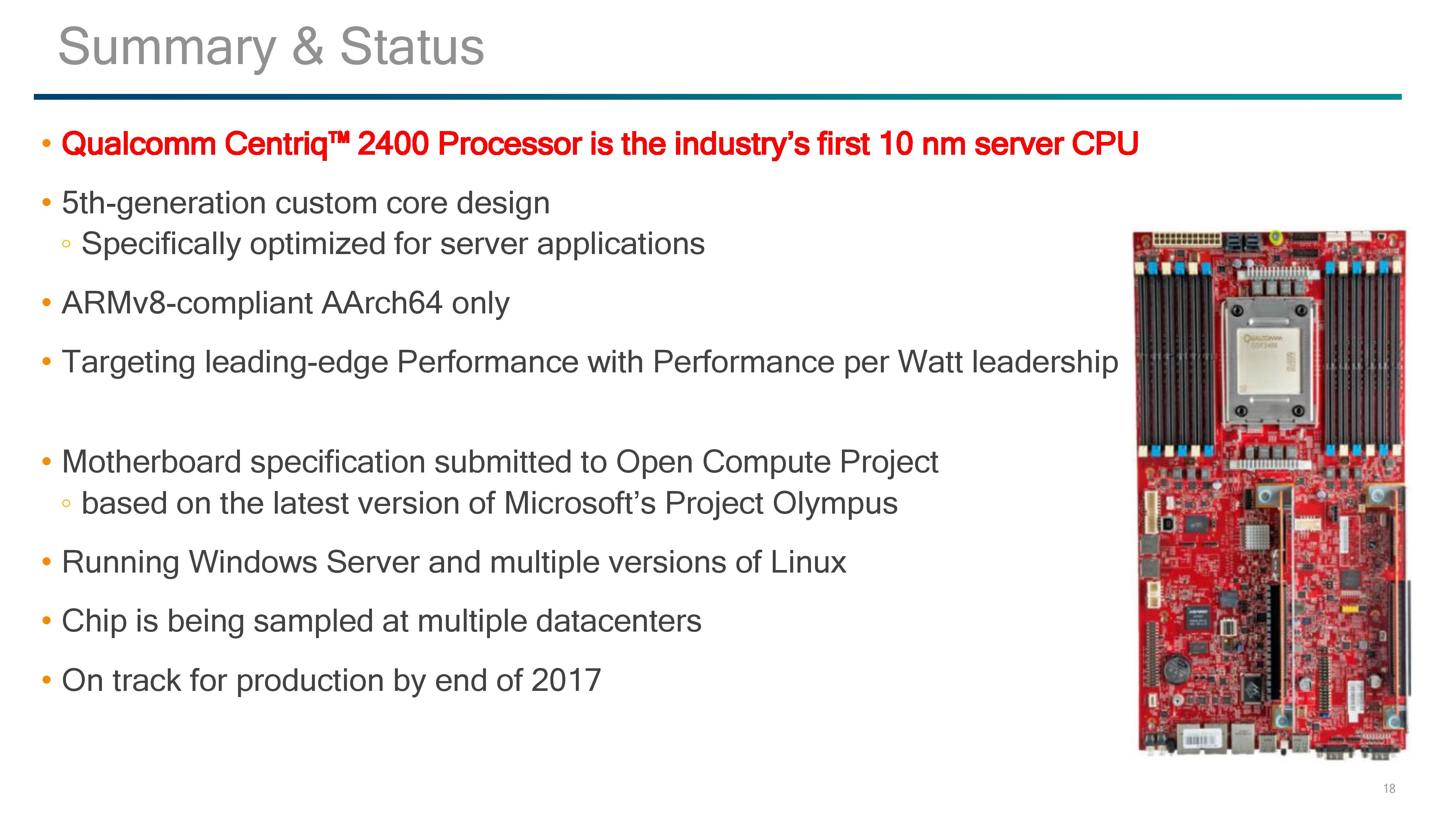
Wrapping thigns up, while Qualcomm has given us more information than we expected, we’d still love to hear exact numbers for L2 and L3 cache sizes, die sizes, TDPs, frequencies (we’ve been told >2.0 GHz with no turbo modes), the different SKUs coming to market, and confirmation about which foundry partner they are using. Qualcomm will also have to be wary about ensuring sufficient support on all operating systems for customers that are interested, especially if this hardware migrates out of the specific customer set that are amenable to testing new platforms.
The Centriq 2400 family is currently being sampled in data centers, and moving into production by the end of 2017. The media sample timeframe unknown, however we're hoping we can get one in for testing before too long.


41 Comments
View All Comments
SarahKerrigan - Sunday, August 20, 2017 - link
I seriously doubt SVE is present. As far as I know, Fujitsu is still lined up to be the first SVE user, and it's not like ultra-wide vectors are a massive boost to conventional enterprise servers.Kevin G - Sunday, August 20, 2017 - link
Using SVE requires ARM v8.2A support which this does not appear to have. The ARM v8.2A spec only was announced in January 2016, which isn't enough time to get it implemented into anything that'd be shipping now. Qualcomm could have been working behind the scenes but that would have given them perhaps another year with a spec that could change before formal publishing (i.e. may require some last minute changes right past the design would be tapping out). For a server part, that path would be unwise.SVE was announced a year ago and is far more complex than the v8.2A released due to how it handles execution width. A SVE design right now is a virtual impossibility.
Hurr Durr - Sunday, August 20, 2017 - link
I`d rather read something on x86 thing on ARM that MS and Qualcomm have than this. Much more potential for the real world.Kevin G - Sunday, August 20, 2017 - link
Can we get an editor in here?"For SoC design followers, one might look at this design and think they see similarities with designs such as AMD’s original Bulldozer design from 2011. ... Actually, after writing that last sentence, it is basically a Xeon Phi dual core module."
While perfectly readable, that last paragraph could use a bit of a rewrite due to the last sentence nullifying it. My quick stab at a rewrite:
For SoC followers, the Qualcomm pairs two modules per fabric stop similar to what Intel has implemented in their most recent Xeon Phi chips. Unlike the new grid topology in the Xeon Phi, Qualcomm is using a ring bus akin to what Intel uses on its Xeon E5 and E7 chips. Those thinking that a dual core module would follow AMD's Bulldozer philosophy will be disappointed to learn that no execution resources are shared between the cores, just the L2 cache, power management and bus interface.
The same comparisons and ideas are made but they flow to the reader a bit more logically to me.
FunBunny2 - Sunday, August 20, 2017 - link
-- Unlike the new grid topology in the Xeon Phi, Qualcomm is using a ring bus akin to what Intel uses on its Xeon E5 and E7 chips.I've long wondered how hardware engineers:
1) discover such alternatives
2) decide which one to choose
Is this fundamental math and physics laws, or trial and error? anyone know a readable (for the non-physics major, that is) source?
Kevin G - Monday, August 21, 2017 - link
Topology has been a well studied concept. At a high level, this mimics general networking design closely. The choice of on-die topology is generally at the mercy of engineering trade offs that are unique in this context.The ring bus you get an easy means of scaling the number of units but the trade of is an increase in latency around the ring bus as the numbers go up. Diminishing returns are hit as the numbers increases. With a ring though, individual units on the ring can be radically different sizes on a die as long the links between stops can be roughly the same for timing purposes. A ring bus also permits a relatively predictable latency to reach stops further away, something noteworthy for implementing coherency protocols. Another trade off with the ring design is that it'll always consume power. Nodes that are not in use still need to have the ring stop going to permit data passage through it.
Qualcomm side steps the ring issue a little bit by including two cores per ring stop, thus putting the minimum number of stops at 24. Just like Intel, I suspect on-die IO like PCIe, memory controllers etc. will have their own ring stops. It is not clear if this all on one massive ring bus or like the last generation of E5/E7 high core count chips, several rings are used with discrete bridges between them. Intel never went beyond 16 ring stops in a design.
A grid topology requires far greater engineering resources to implement correctly. Physical size has to be the same for those nodes in the middle of the grid but there is a bit of wiggle room along the perimeter to expand in one of the two dimensions (handy for things like PCIe, memory controllers that have a fixed need per socket). Cache coherency has to account for variable latency between nodes on the grid: there are several paths to between source and destination. The main benefit of a grid though is that scaling is vastly improved as core count increases. Another benefit is that not all the links in between cores needs to be active to move data. This saves power. Due to the ability to route around congested links, the individual links between grid nodes do not necessarily have to be as wide as those on a ring, saving a bit of energy there while maintaining similar aggregate bandwidth. For servers, multi-pathing of data (ie sending it twice) is also possible for increased RAS if an error in transmit is encountered along a particular path. Intel hasn't indicated that they're doing multipathing but could be a feature they add down the road. In the future if chips stacking emerges outside of research labs as feasible, the grid topology can also expand into the 3rd dimension.
The recent Xeon Phi isn't Intel's first attempt at a grid topology. The first publiclly shown off design was there Terascale research chip a decade ago. ( http://www.eetimes.com/document.asp?doc_id=1303295 ) Inter core topology was a major driver of that research effort and the recent Xeon Phi and Xeon series are the result of those efforts. Intel isn't event the first to implement a grid topology. The Compaq/DEC Alpha EV7 did so between sockets and permitted up to 64 sockets in an 8 x 8 grid from the early 2000's. IBM used a grid-like design for their BlueGene super computer designs to move data, though that wasn't cache coherent. There could be earlier instances as those are a few that I know off hand.
FunBunny2 - Monday, August 21, 2017 - link
thanks. much clearer.Ryan Smith - Sunday, August 20, 2017 - link
Thanks!Lord-Bryan - Sunday, August 20, 2017 - link
"So we have to admit that we were surprised by Qualcomm releasing so much information about the pipeline. When we’ve ever asked the mobile CPU team about Krait and Kryo, we usually hit a brick wall, left with a PR answer of a ‘custom core design’ or the guide of ‘protecting our design"Well am not surprised, releasing architectural details of server cpus, has always been an industry norm. It is something they just have to do if they want to be relevant, you can't just sell black boxes worth thousands of dollars to just anyone.
Lord-Bryan - Sunday, August 20, 2017 - link
Plus developers will have to know how the processor works in other to optimize applications for it, Qualcomm is playing with the big boys now, no room for unnecessary pride.