Analyzing Falkor’s Microarchitecture: A Deep Dive into Qualcomm’s Centriq 2400 for Windows Server and Linux
by Ian Cutress on August 20, 2017 11:00 AM EST- Posted in
- CPUs
- Qualcomm
- Enterprise
- SoCs
- Enterprise CPUs
- ARMv8
- Centriq
- Centriq 2400
Getting Intimate with Falkor: The Back End
The meat and potatoes of Getting Things Done™ is in the core logic – processing instructions with the right data to get the output. The Falkor design has eight of these execution ports: two for load/data, three for ALU/INT, two for FP/vector extensions, and one for direct branches.
The Back End: Load/Store and the L1-Data Cache
The load and store units are usually some of the most vital elements to the design, and here Qualcomm implements 1x128-bit Load and 1x128-bit Store per cycle. Unlike some other competitor designs, there is one unit specifically for load and one specifically for store, rather than issuing two of the same per cycle. These two units have a 3-cycle latency to a hit in the L1-Data cache, which is one cycle faster than most of the competition.
In order to get the latency low, the L1-D cache has to be designed appropriately. So here is a 32KB 8-way design, supporting 64-byte lines but also implementing a write-through strategy. This means that any data committed to L1-D will also be written to the L2. Hardened veterans may recall that the write-through policy was a sizeable bottleneck on AMD’s early Bulldozer designs, so the hope here is that Qualcomm won’t fall into the same trap. The L1-D also supports read-allocate and write-no-allocate modes with split virtual and physical tag addressing.
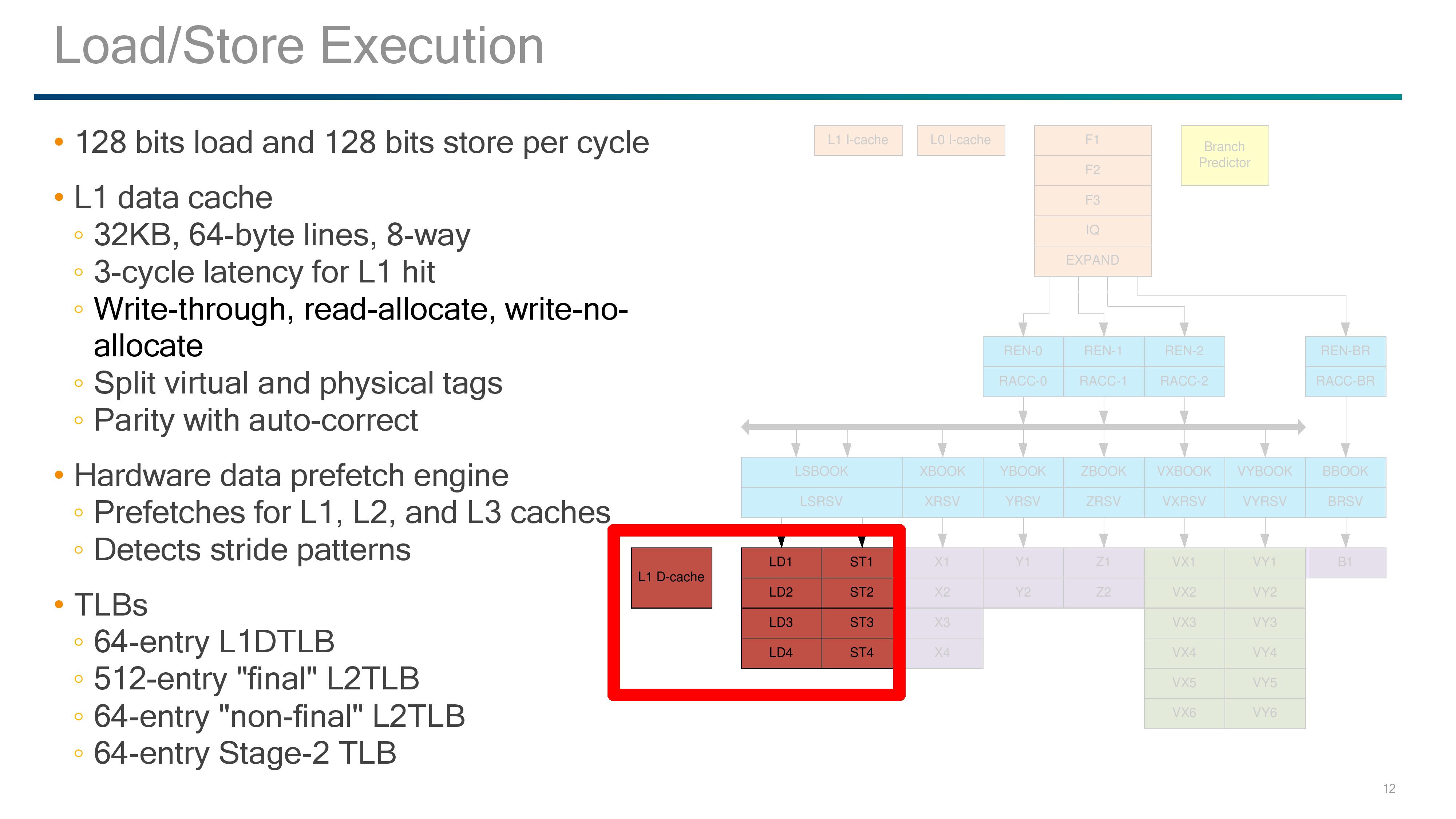
If a miss occurs on the L1-data cache, hardware data prefetchers are used to probe the L2 and L3 caches. Mechanisms are in place to also detect stride pattern access and compensate accordingly. There are two levels of data TLB in place, although as written it comes across as a four-level TLB. It starts with a 64-entry level 1 DTLB, then a larger 512-entry level 2 ‘final’ DTLB. This is backed by a 64-entry level 2 ‘non-final’ DTLB and another 64-entry ‘stage 2’ TLB.
The Back End: ALUs, Vector Extensions, and Branches
On the simple ALU side of the execution ports, Qualcomm labels theses as B, X, Y, and Z-pipes, with a mixed functionality between them and they have different pipeline lengths based on which pipe is needed.
B is for the Branch Pipe, which is for direct branches through the branch side of the decode/rename/queue of the back-end.
The XYZ pipes all perform simple ALU tasks, however only the X pipe can perform MUL operations and takes four stages, and the Z-pipe is the only one for indirect branches. The Y is a simpler ALU-only pipe, with the Y and Z pipe both taking two stages.
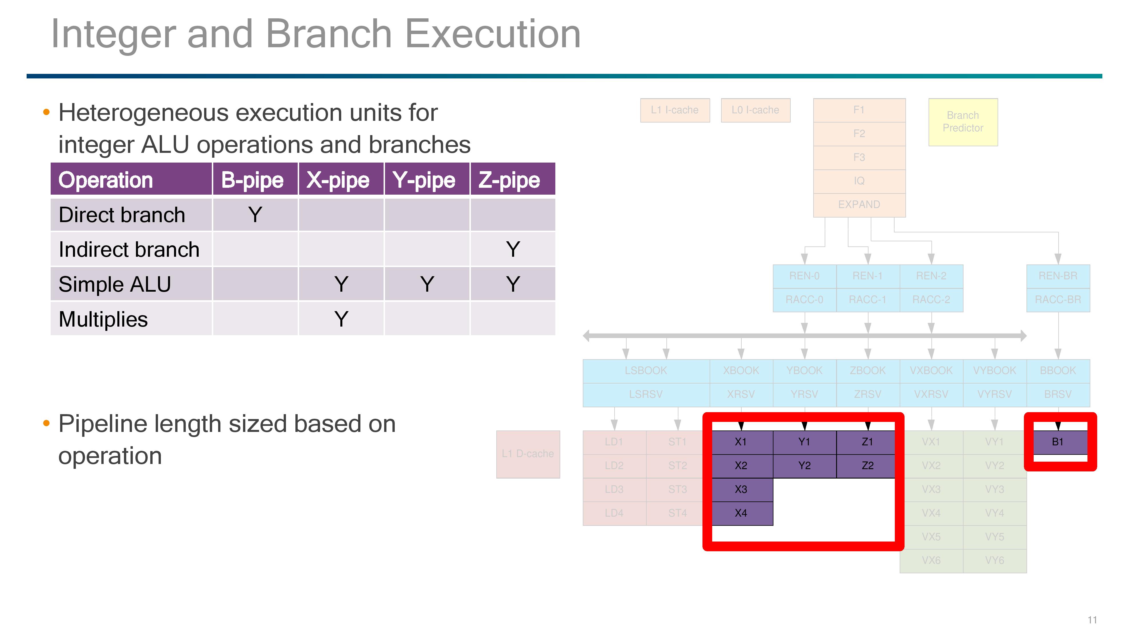
The pipes that Qualcomm did not talk about are the VX and VY pipes, which both come in at six stages each. V in this case likely stands for vectors, and may represent traditional NEON/FP operations found in the smartphone cores in mobile or perhaps the new Vector Extensions (VX?) which ARM introduced last year but have so far not been announced in any commercial product. Vector Extensions would allow for 128-2048 bit wide FP compute, and the idea is that the code required for implementing the vector extensions should be agnostic to how big the vector units actually are. Under ARM’s description, the pipeline should be able to process the data appropriately (although this has a knock on effects for latency if not configured for the ideal vector width).


41 Comments
View All Comments
SarahKerrigan - Sunday, August 20, 2017 - link
I seriously doubt SVE is present. As far as I know, Fujitsu is still lined up to be the first SVE user, and it's not like ultra-wide vectors are a massive boost to conventional enterprise servers.Kevin G - Sunday, August 20, 2017 - link
Using SVE requires ARM v8.2A support which this does not appear to have. The ARM v8.2A spec only was announced in January 2016, which isn't enough time to get it implemented into anything that'd be shipping now. Qualcomm could have been working behind the scenes but that would have given them perhaps another year with a spec that could change before formal publishing (i.e. may require some last minute changes right past the design would be tapping out). For a server part, that path would be unwise.SVE was announced a year ago and is far more complex than the v8.2A released due to how it handles execution width. A SVE design right now is a virtual impossibility.
Hurr Durr - Sunday, August 20, 2017 - link
I`d rather read something on x86 thing on ARM that MS and Qualcomm have than this. Much more potential for the real world.Kevin G - Sunday, August 20, 2017 - link
Can we get an editor in here?"For SoC design followers, one might look at this design and think they see similarities with designs such as AMD’s original Bulldozer design from 2011. ... Actually, after writing that last sentence, it is basically a Xeon Phi dual core module."
While perfectly readable, that last paragraph could use a bit of a rewrite due to the last sentence nullifying it. My quick stab at a rewrite:
For SoC followers, the Qualcomm pairs two modules per fabric stop similar to what Intel has implemented in their most recent Xeon Phi chips. Unlike the new grid topology in the Xeon Phi, Qualcomm is using a ring bus akin to what Intel uses on its Xeon E5 and E7 chips. Those thinking that a dual core module would follow AMD's Bulldozer philosophy will be disappointed to learn that no execution resources are shared between the cores, just the L2 cache, power management and bus interface.
The same comparisons and ideas are made but they flow to the reader a bit more logically to me.
FunBunny2 - Sunday, August 20, 2017 - link
-- Unlike the new grid topology in the Xeon Phi, Qualcomm is using a ring bus akin to what Intel uses on its Xeon E5 and E7 chips.I've long wondered how hardware engineers:
1) discover such alternatives
2) decide which one to choose
Is this fundamental math and physics laws, or trial and error? anyone know a readable (for the non-physics major, that is) source?
Kevin G - Monday, August 21, 2017 - link
Topology has been a well studied concept. At a high level, this mimics general networking design closely. The choice of on-die topology is generally at the mercy of engineering trade offs that are unique in this context.The ring bus you get an easy means of scaling the number of units but the trade of is an increase in latency around the ring bus as the numbers go up. Diminishing returns are hit as the numbers increases. With a ring though, individual units on the ring can be radically different sizes on a die as long the links between stops can be roughly the same for timing purposes. A ring bus also permits a relatively predictable latency to reach stops further away, something noteworthy for implementing coherency protocols. Another trade off with the ring design is that it'll always consume power. Nodes that are not in use still need to have the ring stop going to permit data passage through it.
Qualcomm side steps the ring issue a little bit by including two cores per ring stop, thus putting the minimum number of stops at 24. Just like Intel, I suspect on-die IO like PCIe, memory controllers etc. will have their own ring stops. It is not clear if this all on one massive ring bus or like the last generation of E5/E7 high core count chips, several rings are used with discrete bridges between them. Intel never went beyond 16 ring stops in a design.
A grid topology requires far greater engineering resources to implement correctly. Physical size has to be the same for those nodes in the middle of the grid but there is a bit of wiggle room along the perimeter to expand in one of the two dimensions (handy for things like PCIe, memory controllers that have a fixed need per socket). Cache coherency has to account for variable latency between nodes on the grid: there are several paths to between source and destination. The main benefit of a grid though is that scaling is vastly improved as core count increases. Another benefit is that not all the links in between cores needs to be active to move data. This saves power. Due to the ability to route around congested links, the individual links between grid nodes do not necessarily have to be as wide as those on a ring, saving a bit of energy there while maintaining similar aggregate bandwidth. For servers, multi-pathing of data (ie sending it twice) is also possible for increased RAS if an error in transmit is encountered along a particular path. Intel hasn't indicated that they're doing multipathing but could be a feature they add down the road. In the future if chips stacking emerges outside of research labs as feasible, the grid topology can also expand into the 3rd dimension.
The recent Xeon Phi isn't Intel's first attempt at a grid topology. The first publiclly shown off design was there Terascale research chip a decade ago. ( http://www.eetimes.com/document.asp?doc_id=1303295 ) Inter core topology was a major driver of that research effort and the recent Xeon Phi and Xeon series are the result of those efforts. Intel isn't event the first to implement a grid topology. The Compaq/DEC Alpha EV7 did so between sockets and permitted up to 64 sockets in an 8 x 8 grid from the early 2000's. IBM used a grid-like design for their BlueGene super computer designs to move data, though that wasn't cache coherent. There could be earlier instances as those are a few that I know off hand.
FunBunny2 - Monday, August 21, 2017 - link
thanks. much clearer.Ryan Smith - Sunday, August 20, 2017 - link
Thanks!Lord-Bryan - Sunday, August 20, 2017 - link
"So we have to admit that we were surprised by Qualcomm releasing so much information about the pipeline. When we’ve ever asked the mobile CPU team about Krait and Kryo, we usually hit a brick wall, left with a PR answer of a ‘custom core design’ or the guide of ‘protecting our design"Well am not surprised, releasing architectural details of server cpus, has always been an industry norm. It is something they just have to do if they want to be relevant, you can't just sell black boxes worth thousands of dollars to just anyone.
Lord-Bryan - Sunday, August 20, 2017 - link
Plus developers will have to know how the processor works in other to optimize applications for it, Qualcomm is playing with the big boys now, no room for unnecessary pride.