Analyzing Falkor’s Microarchitecture: A Deep Dive into Qualcomm’s Centriq 2400 for Windows Server and Linux
by Ian Cutress on August 20, 2017 11:00 AM EST- Posted in
- CPUs
- Qualcomm
- Enterprise
- SoCs
- Enterprise CPUs
- ARMv8
- Centriq
- Centriq 2400
Getting Intimate with Falkor: The Back End
The meat and potatoes of Getting Things Done™ is in the core logic – processing instructions with the right data to get the output. The Falkor design has eight of these execution ports: two for load/data, three for ALU/INT, two for FP/vector extensions, and one for direct branches.
The Back End: Load/Store and the L1-Data Cache
The load and store units are usually some of the most vital elements to the design, and here Qualcomm implements 1x128-bit Load and 1x128-bit Store per cycle. Unlike some other competitor designs, there is one unit specifically for load and one specifically for store, rather than issuing two of the same per cycle. These two units have a 3-cycle latency to a hit in the L1-Data cache, which is one cycle faster than most of the competition.
In order to get the latency low, the L1-D cache has to be designed appropriately. So here is a 32KB 8-way design, supporting 64-byte lines but also implementing a write-through strategy. This means that any data committed to L1-D will also be written to the L2. Hardened veterans may recall that the write-through policy was a sizeable bottleneck on AMD’s early Bulldozer designs, so the hope here is that Qualcomm won’t fall into the same trap. The L1-D also supports read-allocate and write-no-allocate modes with split virtual and physical tag addressing.
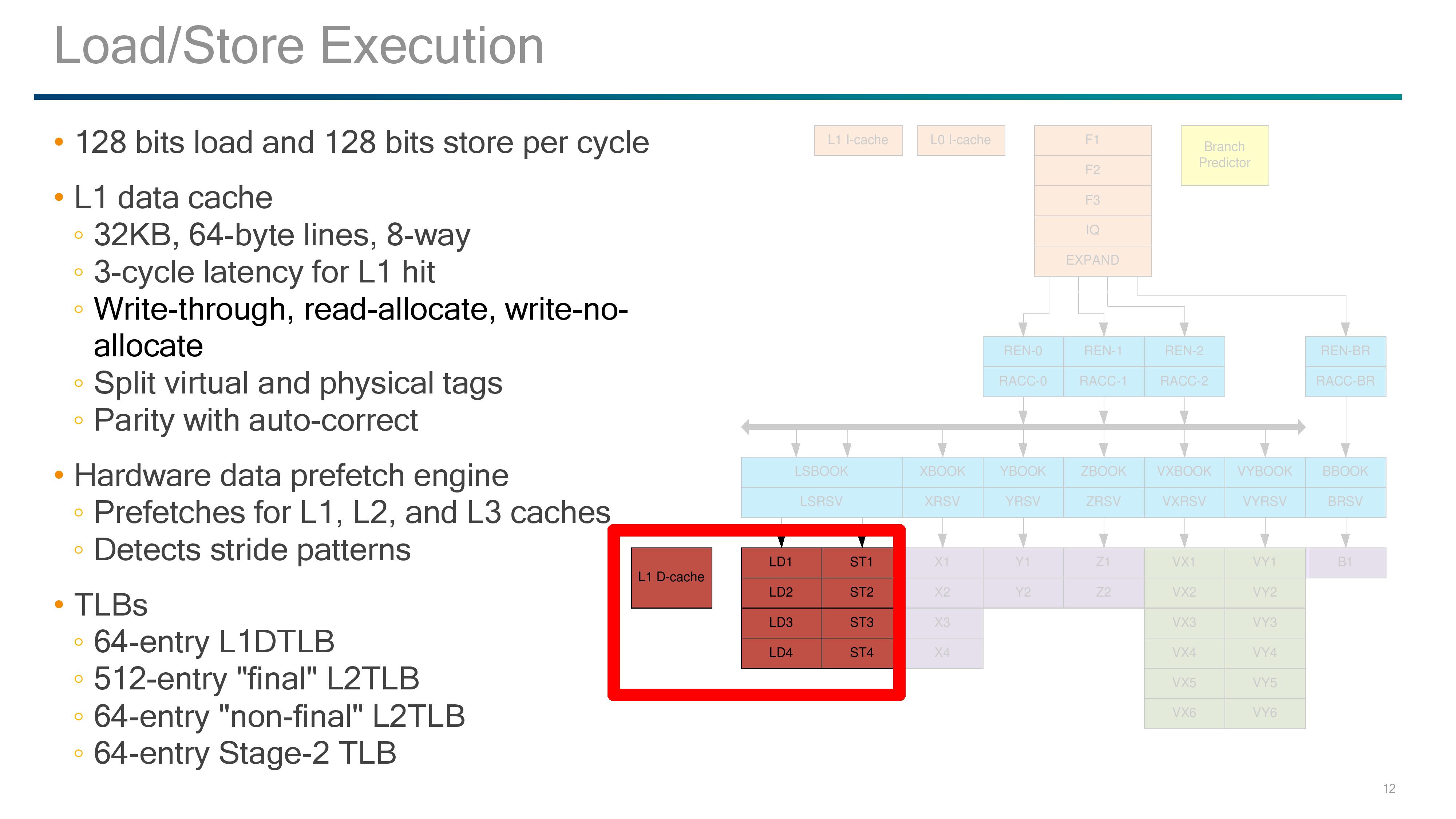
If a miss occurs on the L1-data cache, hardware data prefetchers are used to probe the L2 and L3 caches. Mechanisms are in place to also detect stride pattern access and compensate accordingly. There are two levels of data TLB in place, although as written it comes across as a four-level TLB. It starts with a 64-entry level 1 DTLB, then a larger 512-entry level 2 ‘final’ DTLB. This is backed by a 64-entry level 2 ‘non-final’ DTLB and another 64-entry ‘stage 2’ TLB.
The Back End: ALUs, Vector Extensions, and Branches
On the simple ALU side of the execution ports, Qualcomm labels theses as B, X, Y, and Z-pipes, with a mixed functionality between them and they have different pipeline lengths based on which pipe is needed.
B is for the Branch Pipe, which is for direct branches through the branch side of the decode/rename/queue of the back-end.
The XYZ pipes all perform simple ALU tasks, however only the X pipe can perform MUL operations and takes four stages, and the Z-pipe is the only one for indirect branches. The Y is a simpler ALU-only pipe, with the Y and Z pipe both taking two stages.
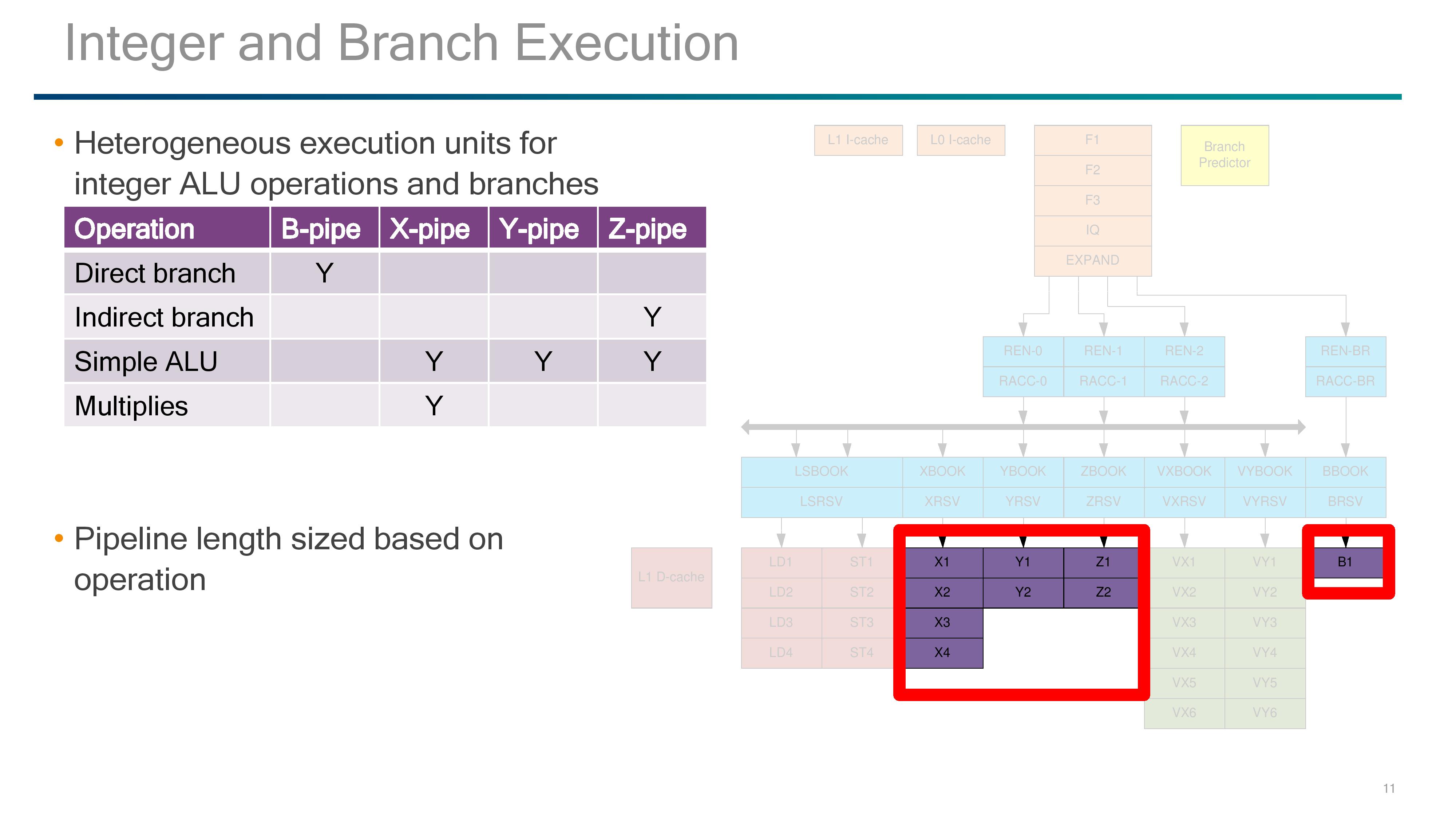
The pipes that Qualcomm did not talk about are the VX and VY pipes, which both come in at six stages each. V in this case likely stands for vectors, and may represent traditional NEON/FP operations found in the smartphone cores in mobile or perhaps the new Vector Extensions (VX?) which ARM introduced last year but have so far not been announced in any commercial product. Vector Extensions would allow for 128-2048 bit wide FP compute, and the idea is that the code required for implementing the vector extensions should be agnostic to how big the vector units actually are. Under ARM’s description, the pipeline should be able to process the data appropriately (although this has a knock on effects for latency if not configured for the ideal vector width).


41 Comments
View All Comments
SarahKerrigan - Sunday, August 20, 2017 - link
"Cavium is the most notable public player using ARM designs in commercial systems so far (there are a number of non-public players focusing on niche scenarios, or whom have little exposure outside of China). The latest design, the Cavium ThunderX2, uses the main A-series core licenses and interconnect license from ARM to provide large numbers of mobile-class CPU cores with as much memory bandwidth and IO as possible."This is not even remotely true. Neither Cavium's cores nor Cavium's interconnect (CCPI predates Cavium's jump to ARM) are ARM IP - they're using an architectural license, *not* IP blocks (or at least, not those ones.) ThunderX uses custom Cavium cores that are between A53 and A57 in performance, while ThunderX2 uses a small number of cores (32) based on the XLP/Vulcan design they bought from Broadcom.
To make that last part more confusing, Cavium initially announced a *different* ThunderX2, which was an enhanced (54-core) derivative of the original ThunderX design. This seems to have been killed when the Vulcan uarch was licensed, or at least has not been heard from since.
Ian Cutress - Sunday, August 20, 2017 - link
That's my fault, I wrote this while flying and thought I had known what is under the hood on ThunderX. Johan actually did a good write up on this, and I'll edit the piece here appropriately.http://www.anandtech.com/show/10353/investigating-...
SarahKerrigan - Sunday, August 20, 2017 - link
"uses the architecture licence for the main A-series core from ARM"That makes even less sense. A-series cores don't factor into it. ThunderX is custom.
name99 - Sunday, August 20, 2017 - link
Is this public knowledge (original ThunderX2 killed, new ThunderX2 based on Vulcan)?I know it's public that (beginning of this year) Cavium acquired Vulcan IP, but I'd not heard anything beyond that. ThunderX2 is supposed to ship Q3 this year (ie RSN...) which to me suggests they're too far along to drop it, and Vulcan will be the basis of ThunderX3.
SarahKerrigan - Sunday, August 20, 2017 - link
Yes. There have been a number of commits to LLVM, etc, indicating that ThunderX2 is now Vulcan. Cf the ThunderX2 LLVM model, which straight-up says "Based on Broadcom Vulcan."I don't know whether the original TX2 design is fully dead or merely mostly dead, but it's pretty obvious at this point that a Vulcan-based TX2 is coming.
SigismundBlack - Sunday, August 20, 2017 - link
Thanks for the info.Denverton rather than 'Denveron'.
Since the C3000 Atom series is cited here re it's also seems worth mentioning AMDs low power server SOCs (e.g. X3421) which likewise feature in recent Moonshot systems and home/SOHO servers.
jameskatt - Sunday, August 20, 2017 - link
The biggest problem I see is if Qualcomm is going to be devoting resources for this project for the long-term. Businesses require stability, predictability, and long-term support. Qualcomm's competitors have been in the business for decades and will be in the business for decades. Qualcomm can't prove they will be in the business for decades to come particularly if they make no money on it.Kevin G - Sunday, August 20, 2017 - link
Qualcomm has been around for awhile so there is stability there. They are new to the ARM server market though because, well after many false starts this market appears to finally be emerging. Even though Qualcomm is just launching this chip, it would be beneficial to them to discuss a roadmap to bring some long term stability to the scene.Wardrive86 - Sunday, August 20, 2017 - link
Surely Qualcomm is using SVE and not regular NEON units. I wish they would expose how wide the units are. I'm very excited they were so open about their architecture. Great write up Ian as well!Dmcq - Sunday, August 20, 2017 - link
I doubt it. SVE is a biggie and was only announced recently, I can't see that Qualcomm would bother risking trying to put it in their first server chip.