The NVIDIA GeForce GTX 1080 & GTX 1070 Founders Editions Review: Kicking Off the FinFET Generation
by Ryan Smith on July 20, 2016 8:45 AM ESTOverclocking
For our final evaluation of the GTX 1080 and GTX 1070 Founders Edition cards, let’s take a look a overclocking.
Whenever I review an NVIDIA reference card, I feel it’s important to point out that while NVIDIA supports overclocking – why else would they include fine-grained controls like GPU Boost 3.0 – they have taken a hard stance against true overvolting. Overvolting is limited to NVIDIA’s built in overvoltage function, which isn’t so much a voltage control as it is the ability to unlock 1-2 more boost bins and their associated voltages. Meanwhile TDP controls are limited to whatever value NVIDIA believes is safe for that model card, which can vary depending on its GPU and its power delivery design.
For GTX 1080FE and its 5+1 power design, we have a 120% TDP limit, which translates to an absolute maximum TDP of 216W. As for GTX 1070FE and its 4+1 design, this is reduced to a 112% TDP limit, or 168W. Both cards can be “overvolted” to 1.093v, which represents 1 boost bin. As such the maximum clockspeed with NVIDIA’s stock programming is 1911MHz.
| GeForce GTX 1080FE Overclocking | ||||
| Stock | Overclocked | |||
| Core Clock | 1607MHz | 1807MHz | ||
| Boost Clock | 1734MHz | 1934MHz | ||
| Max Boost Clock | 1898MHz | 2088MHz | ||
| Memory Clock | 10Gbps | 11Gbps | ||
| Max Voltage | 1.062v | 1.093v | ||
| GeForce GTX 1070FE Overclocking | ||||
| Stock | Overclocked | |||
| Core Clock | 1506MHz | 1681MHz | ||
| Boost Clock | 1683MHz | 1858MHz | ||
| Max Boost Clock | 1898MHz | 2062MHz | ||
| Memory Clock | 8Gbps | 8.8Gbps | ||
| Max Voltage | 1.062v | 1.093v | ||
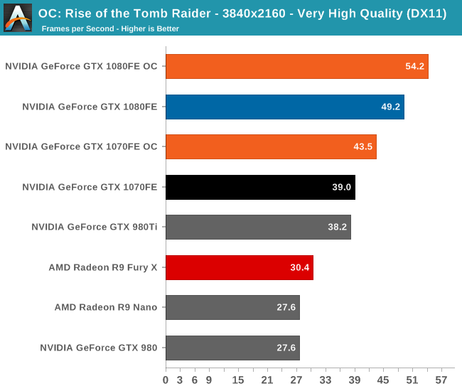
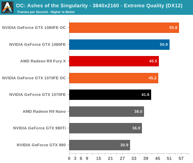
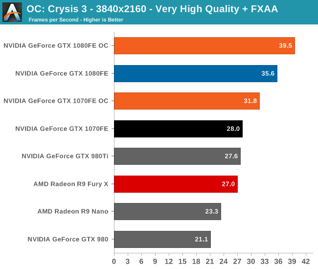
Both cards ended up overclocking by similar amounts. We were able to take the GTX 1080FE another 200MHz (+12% boost) on the GPU, and another 1Gbps (+10%) on the memory clock. The GTX 1070 could be pushed another 175MHz (+10% boost) on the GPU, while memory could go another 800Mbps (+10%) to 8.8Gbps.
Both of these are respectable overclocks, but compared to Maxwell 2 where our reference cards could do 20-25%, these aren’t nearly as extreme. Given NVIDIA’s comments on the 16nm FinFET voltage/frequency curve being steeper than 28nm, this could be first-hand evidence of that. It also indicates that NVIDIA has pushed GP104 closer to its limit, though that could easily be a consequence of the curve.
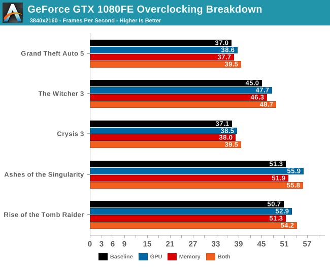
Given that this is our first look at Pascal, before diving into overall performance, let’s first take a look at an overclocking breakdown. NVIDIA offers 4 knobs to adjust when overclocking: overvolting (unlocking additional boost bins), increasing the power/temperature limits, the memory clock, and the GPU clock. Though all 4 will be adjusted for a final overclock, it’s often helpful to see whether it’s GPU overclocking or memory overclocking that delivers the greater impact, especially as it can highlight where the performance bottlenecks are on a card.
To examine this, we’ve gone ahead and benchmarked the GTX 1080 4 times: once with overvolting and increased power/temp limits (to serve as a baseline), once with the memory overclocked added, once with GPU overclock added, and finally with both the GPU and memory overclocks added.
| GeForce GTX 1080 Overclocking Performance | ||||||
| Power/Temp Limit (+20%) | Core (+12%) | Memory (+10%) | Cumulative | |||
| Tomb Raider |
+3%
|
+4%
|
+1%
|
+10%
|
||
| Ashes |
+1%
|
+9%
|
+1%
|
+10%
|
||
| Crysis 3 |
+4%
|
+4%
|
+2%
|
+11%
|
||
| The Witcher 3 |
+2%
|
+6%
|
+3%
|
+10%
|
||
| Grand Theft Auto V |
+1%
|
+4%
|
+2%
|
+8%
|
||
Across all 5 games, the results are clear and consistent: GPU overclocking contributes more to performance than memory overclocking. To be sure, both contribute, but even after compensating for the fact that the GPU overclock was a bit greater than the memory overclock (12% vs 10%), we still end up with the GPU more clearly contributing. Though I am a bit surprised that increasing the power/temperature limit didn't have more of an effect.

Overall we’re looking at an 8%-10% increase in performance from overclocking. It’s enough to further stretch the GTX 1080FE and GTX 1070FE’s leads, but it won’t radically alter performance.
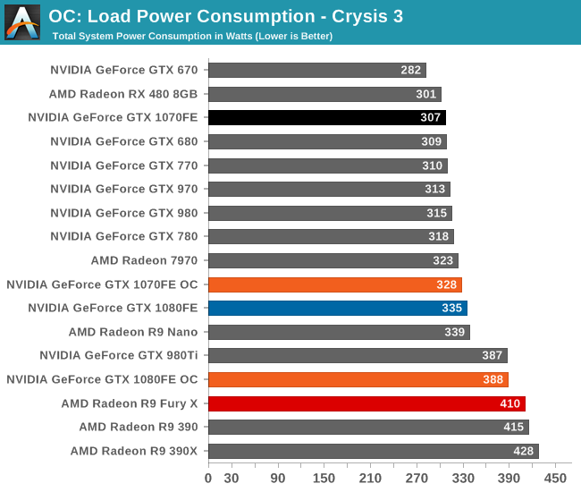
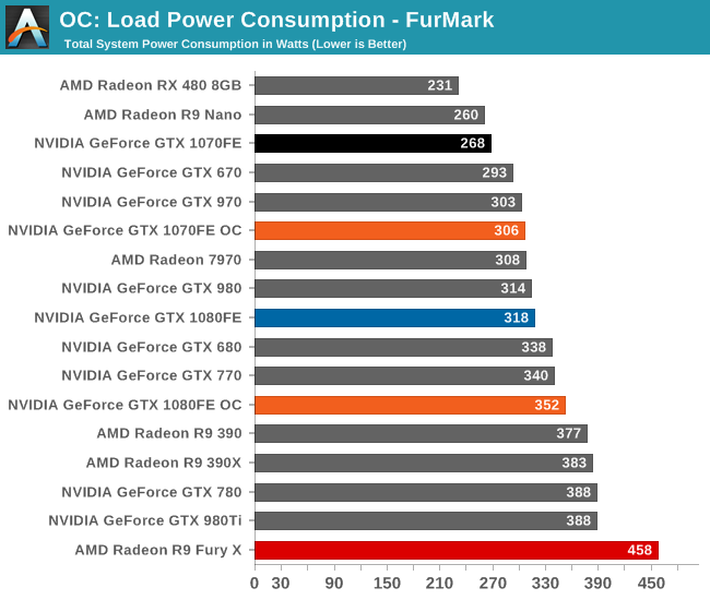
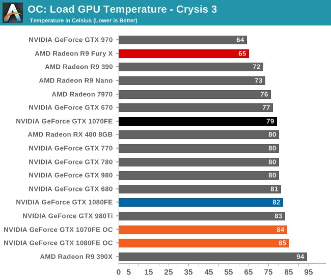
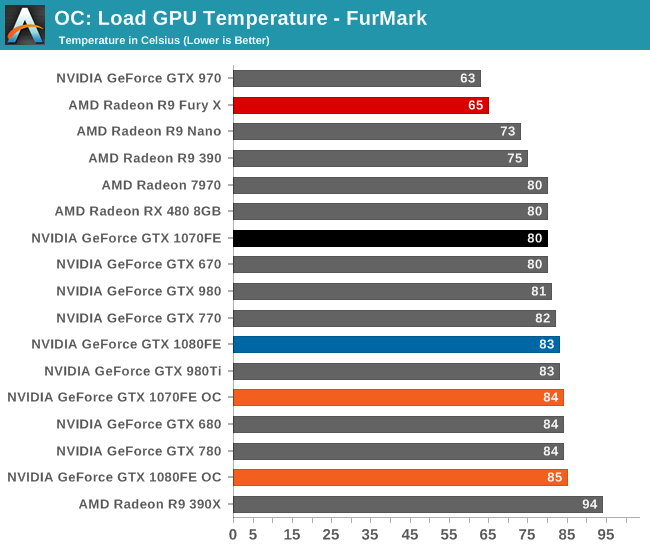
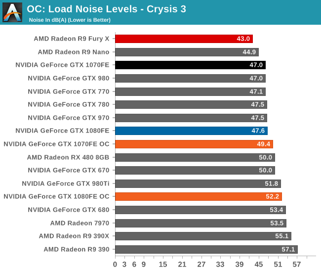
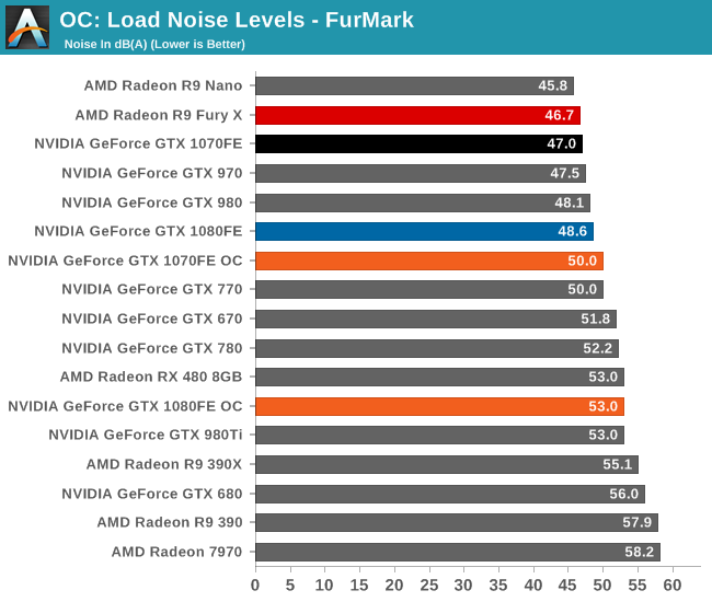
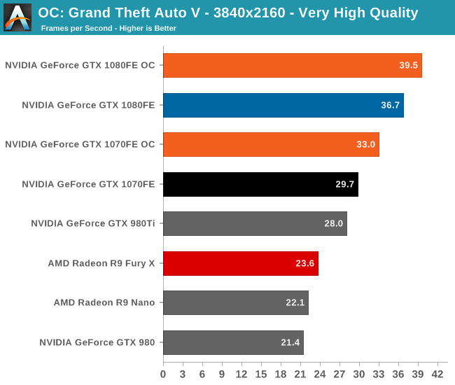
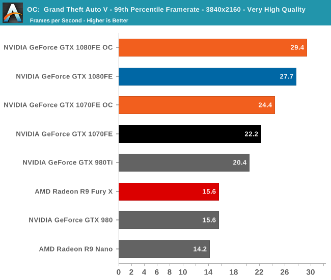
Finally, let’s see the cost of overclocking in terms of power, temperature, and noise. For the GTX 1080FE, the power cost at the wall proves to be rather significant. An 11% Crysis 3 performance increase translates into a 60W increase in power consumption at the wall, essentially moving GTX 1080FE into the neighborhood of NVIDIA’s 250W cards like the GTX 980 Ti. The noise cost is also not insignificant, as GTX 1080FE has to ramp up to 52.2dB(A), a 4.6dB(A) increase in noise. Meanwhile FurMark essentially confirms these findings, with a smaller power increase but a similar increase in noise.
As for the GTX 1070FE, neither the increase in power consumption nor noise is quite as high as GTX 1080FE, though the performance uplift is also a bit smaller. The power penalty is just 21W at the wall for Crysis 3 and 38W for FurMark. This translates to a 2-3dB(A) increase in noise, topping out at 50.0dB for FurMark.


200 Comments
View All Comments
Ryan Smith - Friday, July 22, 2016 - link
2) I suspect the v-sync comparison is a 3 deep buffer at a very high framerate.lagittaja - Sunday, July 24, 2016 - link
1) It is a big part of it. Remember how bad 20nm was?The leakage was really high so Nvidia/AMD decided to skip it. FinFET's helped reduce the leakage for the "14/16"nm node.
That's apples to oranges. CPU's are already 3-4Ghz out of the box.
RX480 isn't showing it because the 14nm LPP node is a lemon for GPU's.
You know what's the optimal frequency for Polaris 10? 1Ghz. After that the required voltage shoots up.
You know, LPP where the LP stands for Low Power. Great for SoC's but GPU's? Not so much.
"But the SoC's clock higher than 2Ghz blabla". Yeah, well a) that's the CPU and b) it's freaking tiny.
How are we getting 2Ghz+ frequencies with Pascal which so closely resembles Maxwell?
Because of the smaller manufacturing node. How's that possible? It's because of FinFET's which reduced the leakage of the 20nm node.
Why couldn't we have higher clockspeeds without FinFET's at 28nm? Because power.
28nm GPU's capped around the 1.2-1.4Ghz mark.
20nm was no go, too high leakage current.
16nm gives you FinFET's which reduced the leakage current dramatically.
What does that enable you to do? Increase the clockspeed..
Here's a good article
http://www.anandtech.com/show/8223/an-introduction...
lagittaja - Sunday, July 24, 2016 - link
As an addition to the RX 480 / Polaris 10 clockspeedGCN2-GCN4 VDD vs Fmax at avg ASIC
http://i.imgur.com/Hdgkv0F.png
timchen - Thursday, July 21, 2016 - link
Another question is about boost 3.0: given that we see 150-200 Mhz gpu offset very common across boards, wouldn't it be beneficial to undervolt (i.e. disallow the highest voltage bins corresponding to this extra 150-200 Mhz) and offset at the same time to maintain performance at lower power consumption? Why did Nvidia not do this in the first place? (This is coming from reading Tom's saying that 1060 can be a 60w card having 80% of its performance...)AnnonymousCoward - Thursday, July 21, 2016 - link
NVIDIA, get with the program and support VESA Adaptive-Sync already!!! When your $700 card can't support the VESA standard that's in my monitor, and as a result I have to live with more lag and lower framerate, something is seriously wrong. And why wouldn't you want to make your product more flexible?? I'm looking squarely at you, Tom Petersen. Don't get hung up on your G-sync patent and support VESA!AnnonymousCoward - Thursday, July 21, 2016 - link
If the stock cards reach the 83C throttle point, I don't see what benefit an OC gives (won't you just reach that sooner?). It seems like raising the TDP or under-voltaging would boost continuous performance. Your thoughts?modeless - Friday, July 22, 2016 - link
Thanks for the in depth FP16 section! I've been looking forward to the full review. I have to say this is puzzling. Why put it on there at all? Emulation would be faster. But anyway, NVIDIA announced a new Titan X just now! Does this one have FP16 for $1200? Instant buy for me if so.Ryan Smith - Friday, July 22, 2016 - link
Emulation would be faster, but it would not be the same as running it on a real FP16x2 unit. It's the same purpose as FP64 units: for binary compatibility so that developers can write and debug Tesla applications on their GeForce GPU.hoohoo - Friday, July 22, 2016 - link
Excellent article, Ryan, thank you!Especially the info on preemption and async/scheduling.
I expected the preemption mght be expensive in some circumstances, but I didn't quite expect it to push the L2 cache though! Still this is a marked improvement for nVidia.
hoohoo - Friday, July 22, 2016 - link
It seems like the preemption is implemented in the driver though? Are there actual h/w instructions to as it were "swap stack pointer", "push LDT", "swap instruction pointer"?