The NVIDIA GeForce GTX 1080 & GTX 1070 Founders Editions Review: Kicking Off the FinFET Generation
by Ryan Smith on July 20, 2016 8:45 AM ESTMeet the GeForce GTX 1080 & GTX 1070 Founders Edition Cards
Now that we’ve had a chance to take a look at all of the architectural features of Pascal, it’s time to get acquainted with the cards themselves.
As I mentioned in the introduction, the GTX 1080 and GTX 1070 Founders Edition cards are a bit of a departure from the norm for NVIDIA. Their actual construction isn’t too significantly changed (more on that in a bit), but NVIDIA has changed how their reference cards by another name are positioned.
In previous generations the reference cards were the baseline; NVIDIA’s board partners could either build higher end cards to sell at higher prices, or build cheaper cards and sell them near the MSRP to capture greater margins. However with the GTX 1000 series, the reference cards have become a higher end option, selling for anywhere between $50 and $100 higher than NVIDIA’s baseline MSRP. This in turn has shifted how NVIDIA’s partners go about pricing their own cards, as they can either price their high-end cards similar to (or more than) the reference card, or undercut NVIDIA’s pricing with their cheaper cards by pricing them closer to the MSRP.
This action has garnered a lot of feedback for NVIDIA, not too much of which has been positive. Ever since GTX Titan in 2013 in particular, NVIDIA’s reference cards have been the card to beat when it comes to blowers. The balance between heat/performance/noise has been finely tuned, and anecdotally speaking, they have proven to be extremely reliable. As a result, the fact that they are now priced as a premium option is vexing for some – myself included – since it moves them farther out of the hands of consumers.
NVIDIA’s rationale for this has been that they see the cards as premium cards and want to price them accordingly. This is no doubt true to an extent – NVIDIA’s reference coolers are not cheap, especially compared to a simple dual fan open air cooler – but on the other hand NVIDIA’s reference PCBs have always been relatively simple, especially compared to overclocking-focused cards. So how premium their reference design actually is will depend on the eye of the beholder.
What isn’t being said by anyone, but I suspect is going on behind the scenes, is that this is a move to help boost margins and satiate the board partners at the same time. It is not a big secret that reference cards fetch the board partners relatively low margins – they have to buy the complete kits from the GPU vendor – which makes them eager to move to semi and fully-custom cards as quickly as they can. By pricing the reference cards above MSRP, this raises the profit margins for everyone. At the same time it means the partners aren’t under quite so much pricing pressure; NVIDIA needs board partners, and it doesn’t do them any good if the partners don’t make any money. Granted, we’re talking about cards that go for upwards of $700, but as these are low volume cards to begin with, the total profits aren’t very high if margins are thin.
In any case, it’s NVIDIA’s hopes that pricing the reference cards over MSRP will also keep them on the market longer. Though due to the current card shortage, we don’t have a good picture of how this is going to play out; demand needs to first slow down to a point where board partners can make some informed decisions about what cards to produce. However, close NVIDIA partners like PNY and EVGA have continued to sell reference cards right up to the end of some model lines in the past, so I’m not convinced that this has really been an issue. But for now it is what it is.
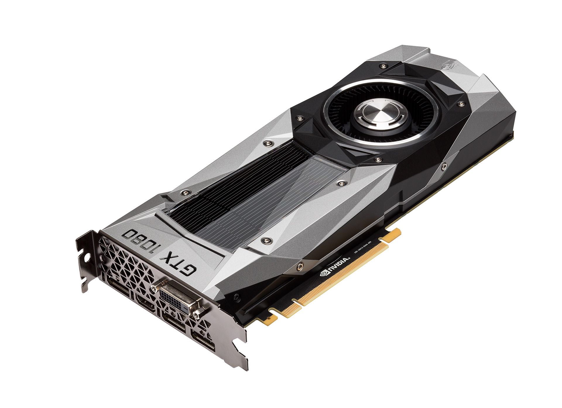
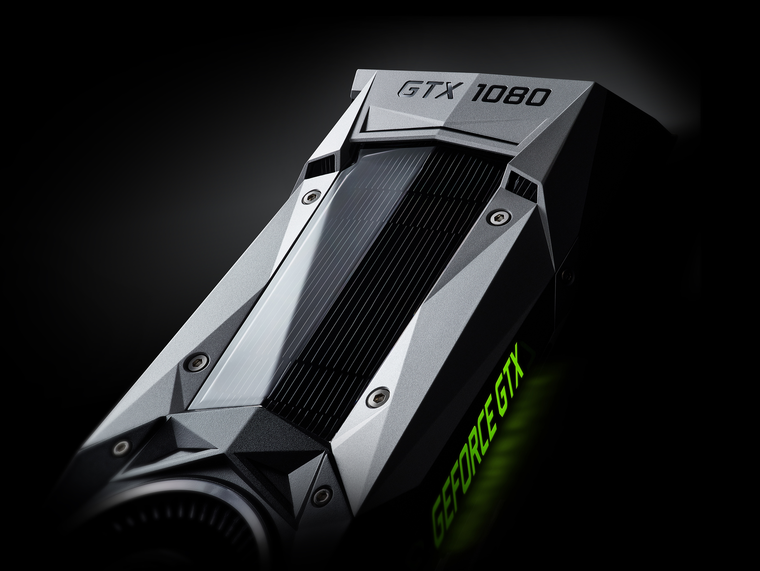
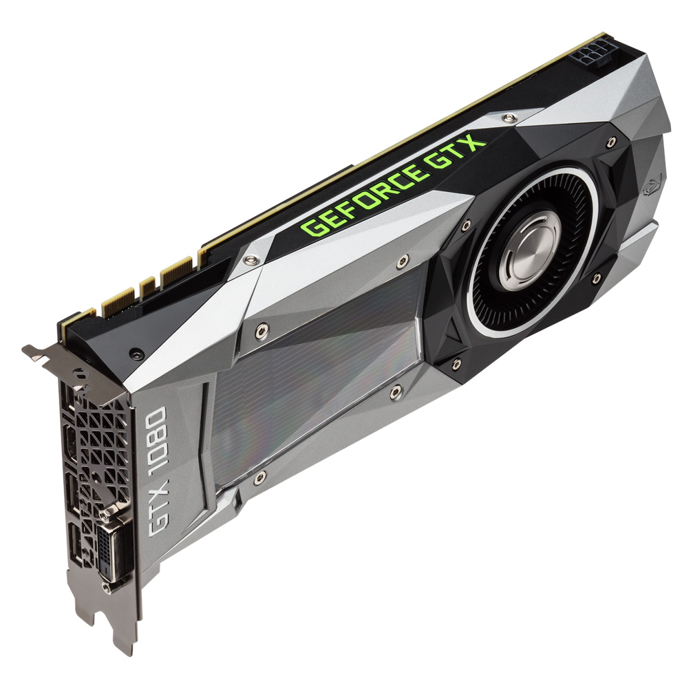
Moving on to the design of the reference boards themselves, if you’ve seen a reference GTX 780/980/Titan card, then at least externally you have a good idea of what to expect. NVIDIA has retained the same basic design of their reference cooler, utilizing a cast aluminum housing and held together using a combination of rivets and screws. NVIDIA has also kept some of the black accenting first introduced by its predecessors, giving the card distinct black tinted polycarbonate window.
The big change here – and one that appears to be almost entire cosmetic – is that NVIDIA has made the shroud more angular. Rather than the largely squared off shroud on the GTX 980 and its ilk, the GTX 1080 and GTX 1070 use a shroud with more intentional triangular cuts. Over the last couple of years NVIDIA has been making triangles a bigger and bigger part of their branding (even Pascal has a triangle connection), and now this has extended over to their reference cards.
Triangles aside, the overall size of the card is unchanged from past reference designs; at 10.5” long, these cards will fit in the same amount of space occupied by past NVIDIA high-end reference cards. The blower design that NVIDIA has come to refine provides a nice balance between cooling and acoustics; it’s not as quiet as a good open air cooler, but because it’s self-exhausting it’s compatible with virtually every case out there, as there’s no need to rely on chassis cooling to handle the heat from the card.
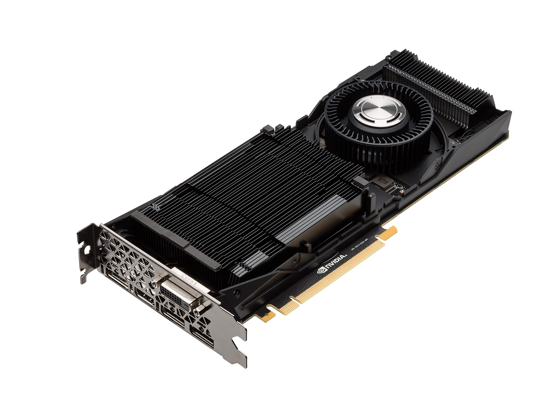
Cracking open the card and removing the shroud exposes the card’s fan and heatsink assembly. Once again NVIDIA is lining the entire card with an aluminum baseplate, which provides heatsinking capabilities for the VRMs and other discrete components below it, along with providing additional protection for the board.
However in a divergence from the reference GTX 980, the reference GTX 1080 adopts the GTX 980 Ti’s vapor chamber cooler for providing heat transfer between the GPU and the heatsink. Vapor chambers are among the highest performing heat transfer mechanisms, which is why they have been used in NVIDIA’s 250W card. The fact that it’s now on the 180W GTX 1080 is due to a combination of factors; the higher price of the card affords more expensive mechanisms like the vapor chamber, and because NVIDIA is straight up maximizing their cooling capabilities for the GTX 1080. Either way, a vapor chamber should not be necessary for a 180W card – and some discussion could be had about just how useful it is – but none the less it gives the GTX 1080 a top-tier cooling system for a blower type card.
Meanwhile the GTX 1070 takes things down one notch. NVIDIA’s 150W card gets a GTX 980-style cooling system, replacing the vapor chamber with a simpler heatpipe based setup. The vapor chamber may very well be overkill for the GTX 1080, but it definitely would be for the GTX 1070, so a heatpipe baseplate setup is still more than enough for a lower power card like the GTX 1070.
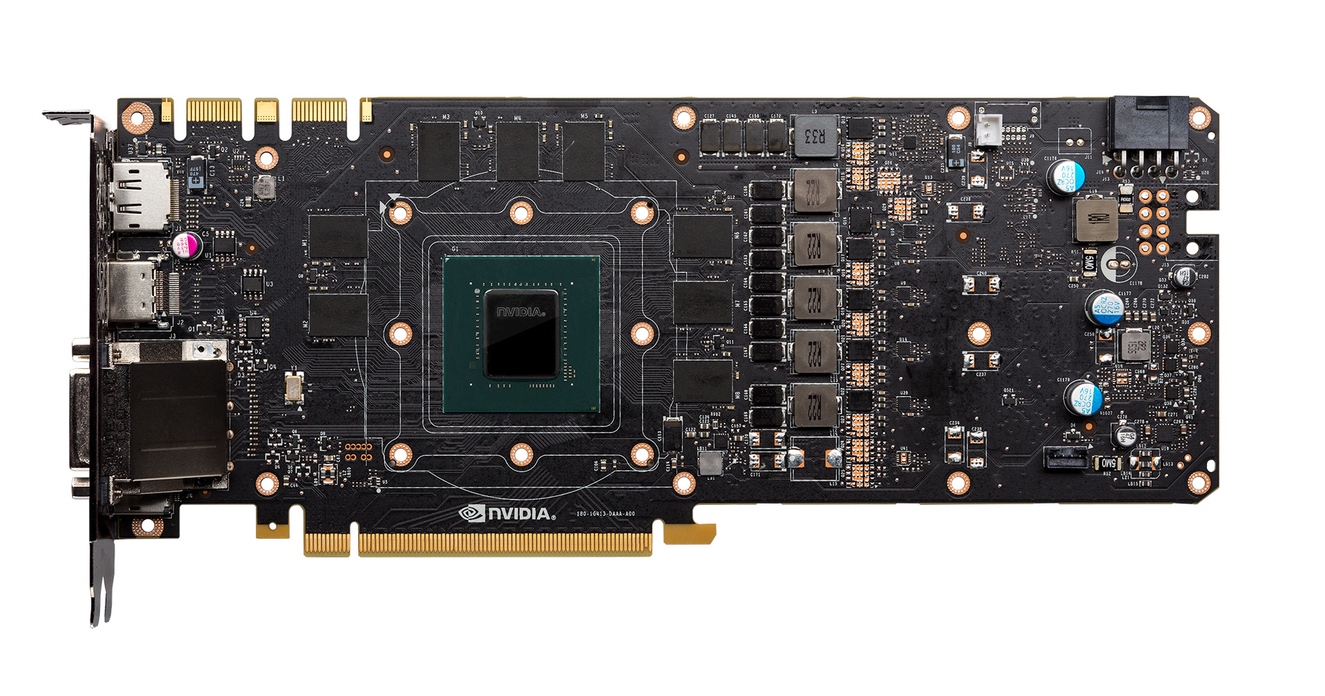
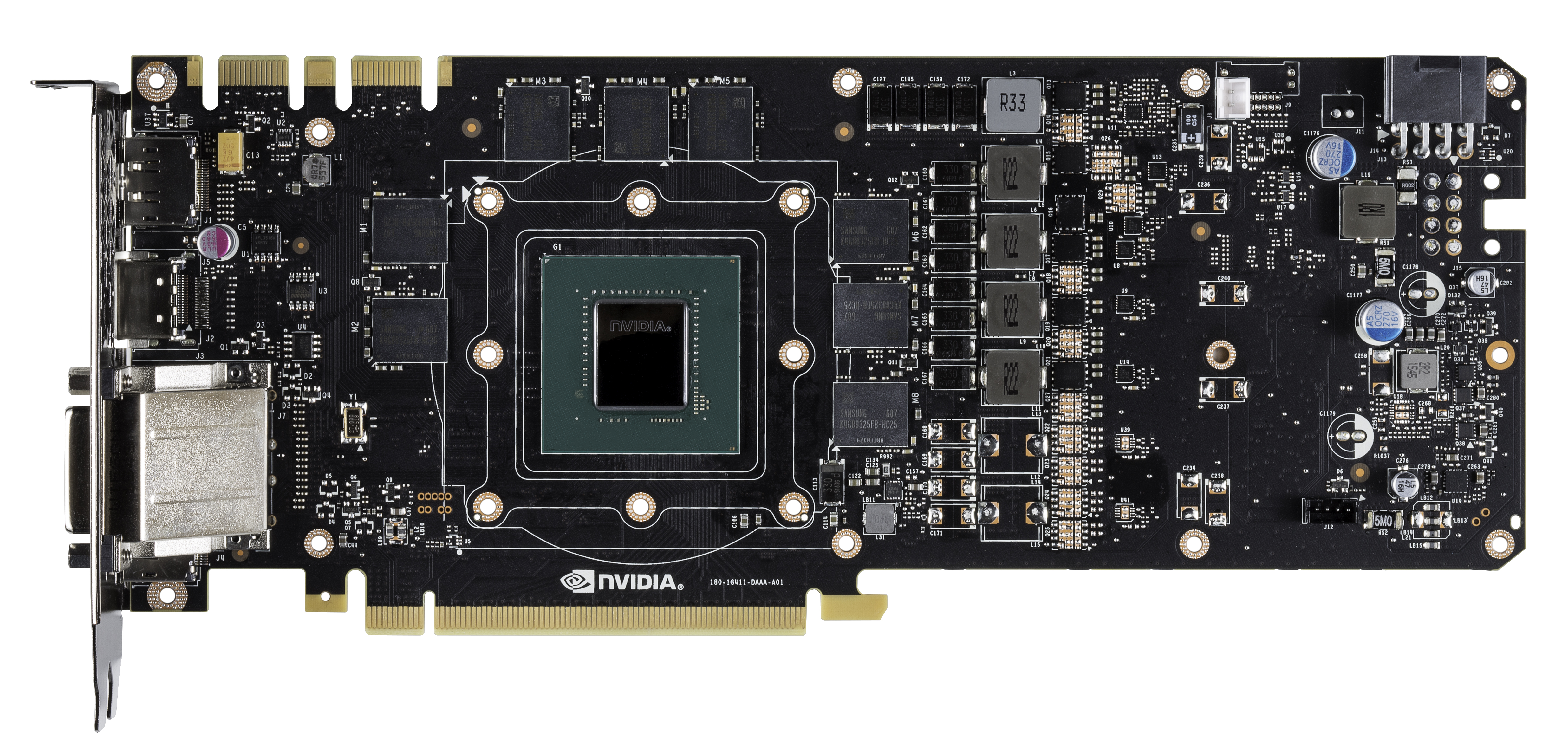
Popping off the cooler, we see NVIDIA’s reference PCB. Unsurprisingly, it’s not too far removed from the reference GTX 980 PCB. At the center we find the GP104 GPU, surrounded by 8 8Gb Micron GDDR5X memory modules, rated for 10Gbps each.
Towards the far side of the PCB we find the card’s power delivery components, which for GTX 1080 is composed of a 5+1 phase design. Here NVIDIA is using 5 power phases for the GPU itself (one more than GTX 980), and then another phase for the GDDR5X. For a 180W card this configuration is more than enough for stock operations and mild overclocking – GTX 1080’s power target limit is 120%, or 216W – however hardcore overclockers will probably end up gravitating towards custom designs more with more heavily overbuilt power delivery systems.
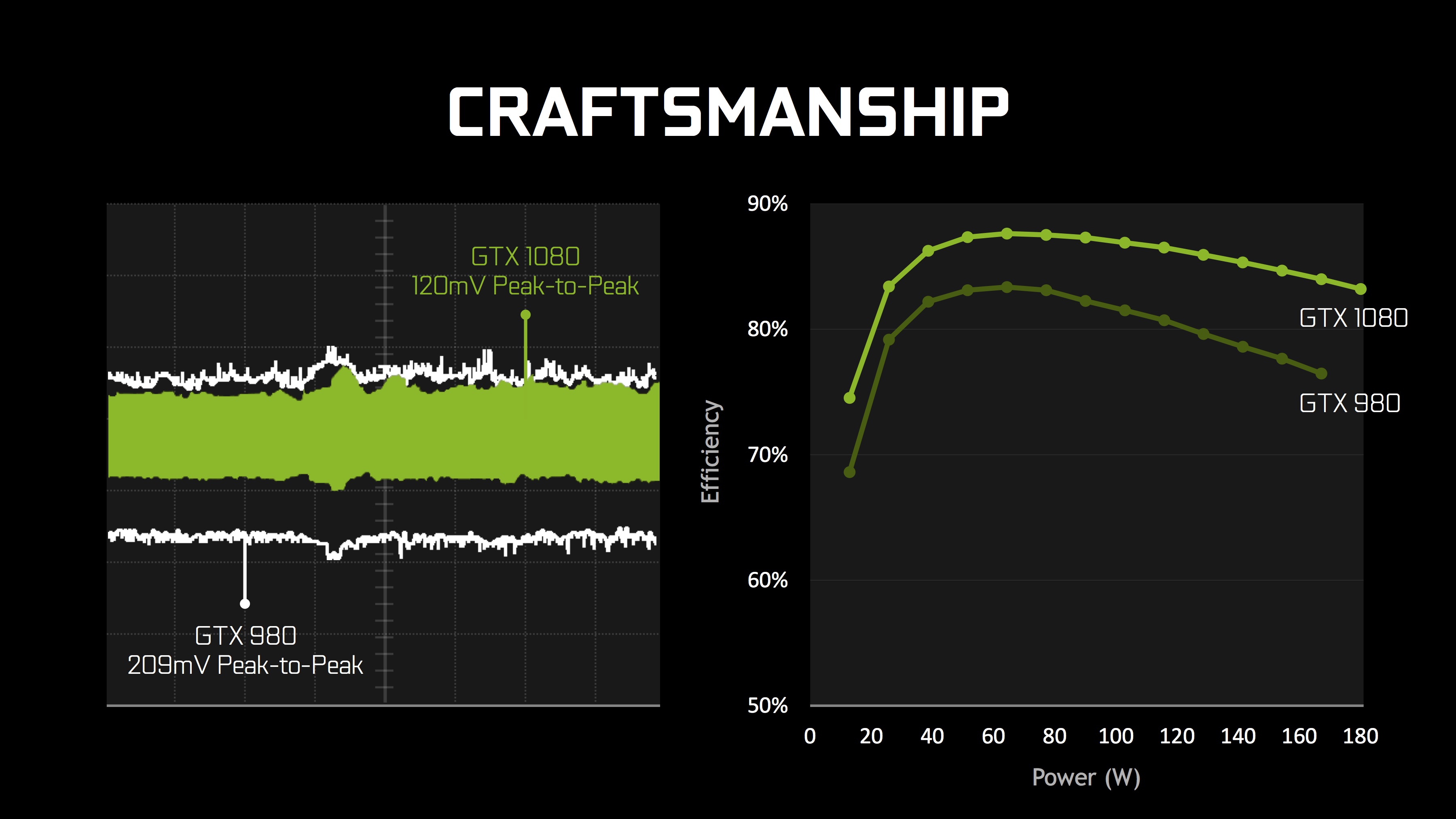
One thing that isn’t immediately evident looking at the PCB is the overall efficiency of the design. One of NVIDIA’s marketing angles for the GTX 1080/GTX 1070 is the craftsmanship of the reference PCB and component selection, which they indicate has tighter tolerances than the GTX 900 series. Among other changes, NVIDIA has been able to reduce peak voltage noise through a combination of dual-FET VRMs and greater filtering by the capacitors. The end result is that NVIDIA is claiming that the GTX 1080’s power delivery circuitry is around 6% more efficient than the GTX 980’s.
Meanwhile for the GTX 1070, we have the same board with a slightly different configuration. Power delivery is down to 4+1, and the Micron GDDR5X has been replaced with standard 8Gbps GDDR5.
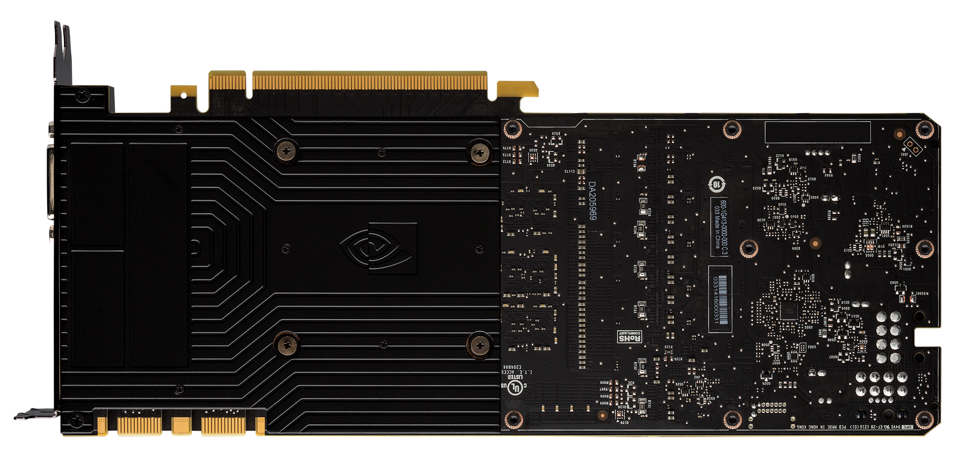
Flipping the card over to the back, we find NVIDIA’s new backplate. The new plate is primarily to protect the backside of the card (there aren’t any major components on the back to cool) and like the GTX 980 before it, includes removable components. The backplate is split into two parts, and either one or both parts can be removed. The idea behind this split is that similar to the GTX 980’s backplate, while the backplate is nice to have, it gets in the way of tightly packed SLI setups. So removing the plate piece directly opposite a fan would give an adjacent card more room to pull in fresh air for cooling purposes.
Moving on, towards the top of the card we find the requisite SLI and power connectors. With the GTX 1000 series NVIDIA has become the latest company to shift from dual 6-pin power connectors to a single 8-pin power connect for cards that need between 150W and 225W. Per the relevant specifications, the power delivery capabilities of the two configurations are identical. But one cable is easier to route and plug in than two, making for slightly cleaner builds and happier technology editors. As for the SLI connectors, as we discussed in our SLI section, these connectors have the same physical interface as the older SLI connectors, but now operate at up to 650MHz on Pascal. A recent LED bridge – or better still, the new HB bridge – is necessary to get the best performance out of SLI with these cards.
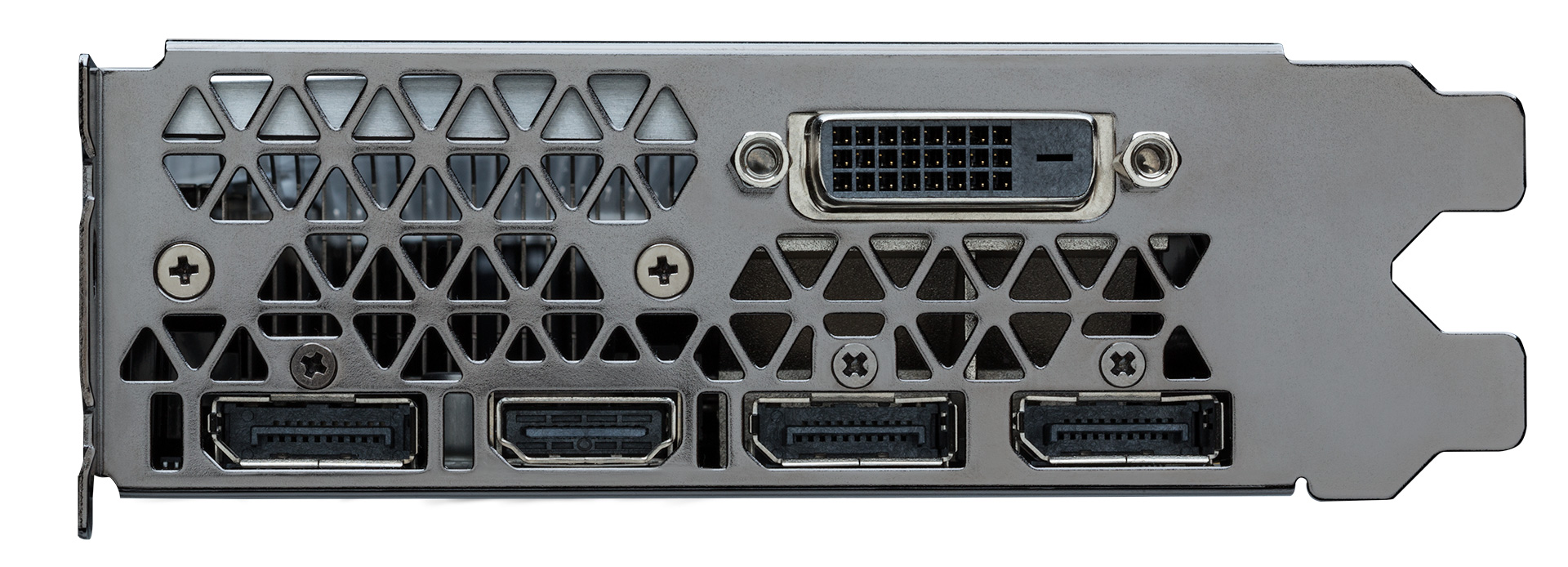
Meanwhile, looking at NVIDIA’s display I/O configuration, it’s physically unchanged from prior reference cards. What’s new here is that Pascal supports the newer DisplayPort 1.3/1.4 standards, along with HDMI 2.0b. This means we’re looking at 3x DisplayPort 1.3/1.4, 1x HDMI 2.0b, and 1x DL-DVI-D. The latter is also a change from GTX 980, as NVIDIA has gone from a digital + analog DVI port to a pure digital DVI port. So if for whatever reason you wanted to hook up an analog monitor to a $400+ video card, you will need a DisplayPort to VGA adapter, as GTX 1080/1070 do not provide a native analog output.
It should also be noted that as the physical port arrangements haven’t changed in a generation, neither have the underlying display capabilities. Like Maxwell 2 before it, Pascal supports up to 4 displays, which can be muxed among 6 display outputs.


200 Comments
View All Comments
Ryan Smith - Friday, July 22, 2016 - link
2) I suspect the v-sync comparison is a 3 deep buffer at a very high framerate.lagittaja - Sunday, July 24, 2016 - link
1) It is a big part of it. Remember how bad 20nm was?The leakage was really high so Nvidia/AMD decided to skip it. FinFET's helped reduce the leakage for the "14/16"nm node.
That's apples to oranges. CPU's are already 3-4Ghz out of the box.
RX480 isn't showing it because the 14nm LPP node is a lemon for GPU's.
You know what's the optimal frequency for Polaris 10? 1Ghz. After that the required voltage shoots up.
You know, LPP where the LP stands for Low Power. Great for SoC's but GPU's? Not so much.
"But the SoC's clock higher than 2Ghz blabla". Yeah, well a) that's the CPU and b) it's freaking tiny.
How are we getting 2Ghz+ frequencies with Pascal which so closely resembles Maxwell?
Because of the smaller manufacturing node. How's that possible? It's because of FinFET's which reduced the leakage of the 20nm node.
Why couldn't we have higher clockspeeds without FinFET's at 28nm? Because power.
28nm GPU's capped around the 1.2-1.4Ghz mark.
20nm was no go, too high leakage current.
16nm gives you FinFET's which reduced the leakage current dramatically.
What does that enable you to do? Increase the clockspeed..
Here's a good article
http://www.anandtech.com/show/8223/an-introduction...
lagittaja - Sunday, July 24, 2016 - link
As an addition to the RX 480 / Polaris 10 clockspeedGCN2-GCN4 VDD vs Fmax at avg ASIC
http://i.imgur.com/Hdgkv0F.png
timchen - Thursday, July 21, 2016 - link
Another question is about boost 3.0: given that we see 150-200 Mhz gpu offset very common across boards, wouldn't it be beneficial to undervolt (i.e. disallow the highest voltage bins corresponding to this extra 150-200 Mhz) and offset at the same time to maintain performance at lower power consumption? Why did Nvidia not do this in the first place? (This is coming from reading Tom's saying that 1060 can be a 60w card having 80% of its performance...)AnnonymousCoward - Thursday, July 21, 2016 - link
NVIDIA, get with the program and support VESA Adaptive-Sync already!!! When your $700 card can't support the VESA standard that's in my monitor, and as a result I have to live with more lag and lower framerate, something is seriously wrong. And why wouldn't you want to make your product more flexible?? I'm looking squarely at you, Tom Petersen. Don't get hung up on your G-sync patent and support VESA!AnnonymousCoward - Thursday, July 21, 2016 - link
If the stock cards reach the 83C throttle point, I don't see what benefit an OC gives (won't you just reach that sooner?). It seems like raising the TDP or under-voltaging would boost continuous performance. Your thoughts?modeless - Friday, July 22, 2016 - link
Thanks for the in depth FP16 section! I've been looking forward to the full review. I have to say this is puzzling. Why put it on there at all? Emulation would be faster. But anyway, NVIDIA announced a new Titan X just now! Does this one have FP16 for $1200? Instant buy for me if so.Ryan Smith - Friday, July 22, 2016 - link
Emulation would be faster, but it would not be the same as running it on a real FP16x2 unit. It's the same purpose as FP64 units: for binary compatibility so that developers can write and debug Tesla applications on their GeForce GPU.hoohoo - Friday, July 22, 2016 - link
Excellent article, Ryan, thank you!Especially the info on preemption and async/scheduling.
I expected the preemption mght be expensive in some circumstances, but I didn't quite expect it to push the L2 cache though! Still this is a marked improvement for nVidia.
hoohoo - Friday, July 22, 2016 - link
It seems like the preemption is implemented in the driver though? Are there actual h/w instructions to as it were "swap stack pointer", "push LDT", "swap instruction pointer"?