AMD's Graphics Core Next Preview: AMD's New GPU, Architected For Compute
by Ryan Smith on December 21, 2011 9:38 PM ESTPrelude: The History of VLIW & Graphics
Before we get into the nuts & bolts of Graphics Core Next, perhaps it’s best to start at the bottom, and then work our way up.
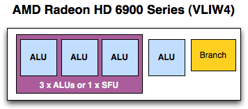
The fundamental unit of AMD’s previous designs has been the Streaming Processor, previously known as the SPU. In every modern AMD design other than Cayman (6900), this is a Very Long Instruction Word 5 (VLIW5) design; Cayman reduced this to VLIW4. As implied by the architectural name, each SP would in turn have 5 or 4 fundamental math units – what AMD now calls Radeon cores – which executed the individual instructions in parallel over as many clocks as necessary. Radeon cores were coupled with registers, a branch unit, and a special function (transcendental) unit as necessary to complete the SP.
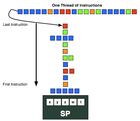
VLIW designs are designed to excel at executing many operations from the same task in parallel by breaking it up into smaller groupings called wavefronts. In AMD’s case a wavefront is a group of 64 pixels/values and the list of instructions to be executed against them. Ideally, in a wavefront a group of 4 or 5 instructions will come down the pipe and be completely non-interdependent, allowing every Radeon core to be fed. When dependent instructions would come down however, fewer instructions could be scheduled at once, and in the worst case only a single instruction could be scheduled. VLIW designs will never achieve perfect efficiency in this regard, but the farther real world utilization is from ideal efficiency, the weaker the benefits of VLIW.
The use of VLIW can be traced back to the first AMD DX9 GPU, R300 (Radeon 9700 series). If you recall our Cayman launch article, we mentioned that AMD initially used a VLIW design in those early parts because it allowed them to process a 4 component dot product (e.g. w, x, y, z) and a scalar component (e.g. lighting) at the same time, which was by far the most common graphics operation. Even when moving to unified shaders in DX10 with R600 (Radeon HD 2900), AMD still kept the VLIW5 design because the gaming market was still DX9 and using those kinds of operations. But as new games and GPGPU programs have come out efficiency has dropped over time, and based on AMD’s own internal research at the time of the Cayman launch the average shader program was utilizing only 3.4 out of 5 Radeon cores. Shrinking from VLIW5 to VLIW4 fights this some, but utilization will always be a concern.
Finally, it’s worth noting what’s in charge of doing all of the scheduling. In the CPU world we throw things at the CPU and let it schedule actions as necessary – it can even go out-of-order (OoO) within a thread if it will be worth it. With VLIW, scheduling is the domain of the compiler. The compiler gets the advantage of knowing about the full program ahead of time and can intelligently schedule some things well in advance, but at the same time it’s blind to other conditions where the outcome is unknown until the program is run and data is provided. Because of this the schedule is said to be static – it’s set at the time of compilation and cannot be changed in-flight.
So why in an article about AMD Graphics Core Next are we going over the quick history of AMD’s previous designs? Without understanding the previous designs, we can’t understand what is new about what AMD is doing, or more importantly why they’re doing it.


83 Comments
View All Comments
StormyParis - Friday, June 17, 2011 - link
Thank you for a very enlightening write up. Comments and questions:1- please add a comma in there somewhere. I had to read the sentence 4 times to understand it (page 1=: "VLIW designs will never achieve perfect efficiency in this regard, but the farther off real world utilization is the weaker the benefits of VLIW."
2- When, if ever, will we vile users see any benefits ? I get the feeling that most apps are still not optimized well, if at all, for multicore/threading. Come to think of it, most don't even use most of the x86 extensions more recent than SSE2. Now we're talking of yet another x86 extension, that is not only AMD-specific, but very task-specific. Apart from a handful of labs doing GPU computing, and the usual Photoshop filters... i'm doubtful ?
MonkeyPaw - Friday, June 17, 2011 - link
I'm not an expert in this sort of design, but is AMD setting up this architecture to replace the x86 ALU? Bulldozer is already running 2 ALUs for every 1 FPU, which is promoting ALU-heavy software design. It may take a few revisions to meld them (or phase one out), but it certainly seems like that's a heterogeneous CPU in the end.marc1000 - Friday, June 17, 2011 - link
there is a slide (on Llano article, I believe) where AMD points this. yes, they want to completely merge them, and the ALU would be one of this mergind points.A5 - Friday, June 17, 2011 - link
I think it'll be quite awhile before the monolithic cores dissolve into the heterogeneous architectures, mostly depending on how fine-grained the power gating can get. When it gets to the point where the CPU can selectively turn off components inside a given SIMD unit, I think we'll see someone go "Wait a minute, then why do we even have this big core anymore?" and it'll go away. 2018ish, maybe?jamescox - Monday, June 20, 2011 - link
ALU is generally used to refer to a very simple unit that performs arithmetic, logic, and possibly bit shift operations on integers, not floating point values. The units labeled ALU in the GPU diagrams in the article may support some integer operations, but they mainly process 32-bit floating point values, and (IMO) should not be labeled as "ALUs". FPU would probably be more accurate, but I do not know what operations these units support and whether they include a native integer ALU or just convert to integers to FP.
I don't know what you would mean by ALU-heavy software design. Bulldozer has two integer execution cores per module. Each core is composed of 2 ALUs and 2 AGUs, not shared. It also has 2 128-bit floating point (FMA) units per module shared between the two threads. This isn't really much different than an intel hyper-threaded core. Intel has, I believe, 3 ALUs, 3 AGUs, and 2 FPUs per core which is shared between 2 threads. AMDs version of multi-threading just doesn't share as much hardware between threads, which may be better than Intel's HT (2-2-1 AMD vs 1.5-1.5-1 Intel ALU-AGU-FPU). Intel's version would allow a single thread to us all of the execution resources at once, if there is no competing thread. Sharing the FPU makes a lot of sense, since most code that runs on CPUs only uses the FPU intermittently. If the code uses FP more than intermittently, then it would be a candidate for vectorization, and execution on the GPU instead.
While AMDs next generation graphics hardware may be able to execute more general code compiled from a wider range of languages, it is not an x86 processor, and it can not replace the CPU. If you look at the diagram, it has a single scalar unit to handle non-vector code in each compute unit. It also has 64 units in the 4 vector arrays of each CU. If you actually tried to compile and run the kind of branch heavy, integer code that CPUs have to deal with on a CU, then it would probably run entirely and very, very slowly on that single scalar unit.
MrSpadge - Wednesday, June 22, 2011 - link
I think you've got the right idea with this being melted into a Bulldozer-like design. however, it wouldn't replace the x86 ALUs, which are highly-optimized for high clock speed and low latency execution, as well as excellent handling of branches etc.No, it would rather replace or supplement a fat FPU shared between many "cores" (which, by then would basically mean ALUs + scheduling). Most tasks which requires massive fp number crunching can be executed well in parallel and therefore are suitable for execution on a GPU core. The question is just how to bond them together so that the software guys can actually use them..
MrS
Deleted - Thursday, December 22, 2011 - link
Basically, what we have here is a math coprocessor. Back in the day, Intel's x86 processors were very good (relatively speaking) at integer math, but choked on floating point math. So Intel created the 8087 to handle the floating point calculations while the CPU handled the integer calculations (obviously this wasn't exclusive to Intel, but I'm generalizing). Eventually, the floating point unit was merged onto the CPU, and programs began using them interchangeably.What we have today is very similar. CPUs, even with their advanced FPUs, are nowhere near as powerful as the massively parallel monstrosities we use for graphics. Eventually, they will be merged onto the CPU, and used as readily for general floating point processing tasks as FPUs are currently.
And this is the point of Fusion: to fully replace the aging floating point unit with an IGP.
A5 - Friday, June 17, 2011 - link
The benefits to home or enthusiast users of heterogeneous CPUs are still several years off. We need market penetration of hardware along with fundamental changes in software development models and smarter compilers.nedwards - Tuesday, January 28, 2014 - link
Smarter programmers would help! Let me rephrase that. Programmers thinking in a parallel mindset would help!Beenthere - Friday, June 17, 2011 - link
If AMD delivers in a timely manner they will have a bright future. This looks like a huge technological transition and I understand the need to get developers onboard now but it also tips AMD's hand to Intel who will steal any ideas that they can.Unfortunately we are still waiting for most applications to be written for 64-bit use so I'm not holding out much hope for an expeditious migration on a complex technological transition though it does appear that maybe AMD has been working on this for some time and may be able to do a better job of executing with Trinity and future products. Time will tell but I hope AMD delivers on time and they will definitely get my dime - all of them.