Supermicro Shows Off Intel Nervana NNP-T Servers: 8-Way PCIe and OAM
by Dr. Ian Cutress on December 4, 2019 3:00 PM EST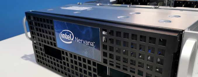
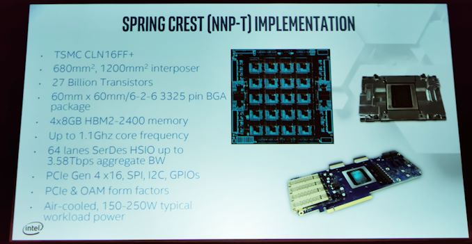
One of the key elements to deep learning and training is lots of very dense compute, as well as the dense servers to go through the computation. Intel’s Nervana NNP-T Spring Crest silicon, which we saw at Hot Chips earlier this year, is the ‘big training silicon’ that came out of the acquisition with Nervana: a 680 mm2 built on TSMC 16nm with CoWoS with four stacks of HBM2. The servers using this silicon are now starting to appear, and we caught sight of two at the Supermicro booth at Supercomputing.
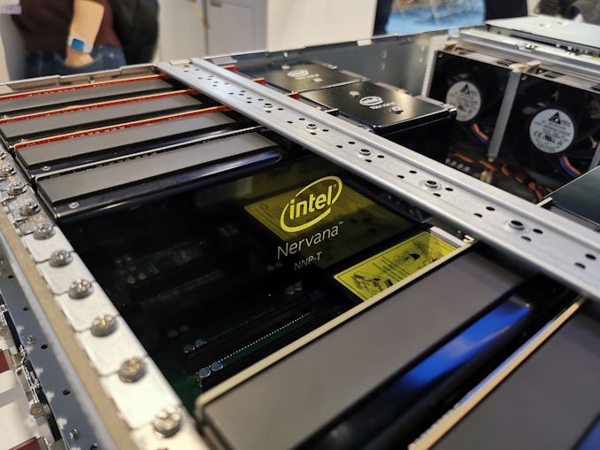
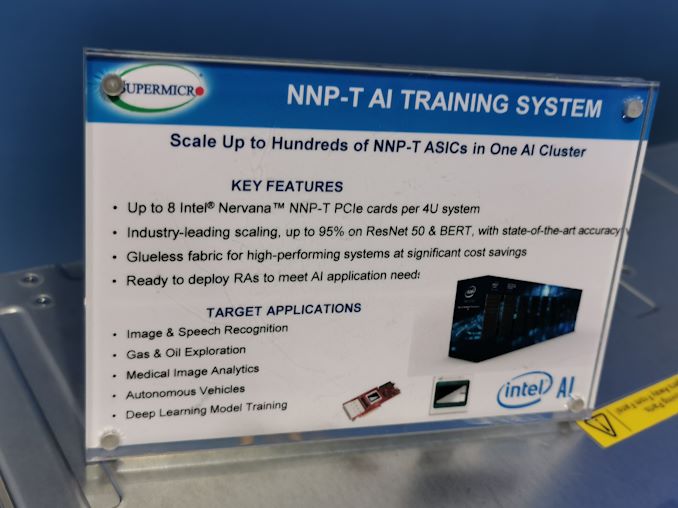
To start the week, Supermicro showed off its first server using the NNP-T hardware, all based on PCIe cards. As one might imagine, these fit into any server that was previously designed to accommodate GPUs, and so Supermicro’s system is a very typical 2P unit with 8 cards in a 4U design. The cards talk to each other, with 3.58 Tbps total bi-directional bandwidth per chip, and off-chip connections supporting scalability up to 1024 nodes. As noted by the single 8-pin PCIe power per card, it means that each card has a peak power of 225W as per PCIe standards.
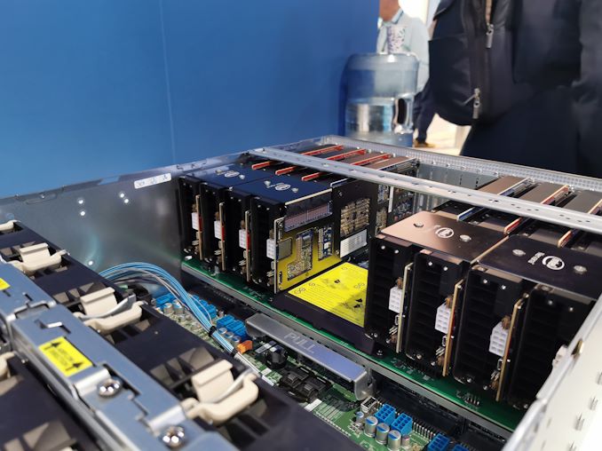
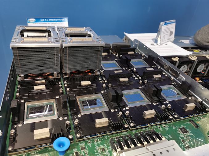
Later in the week, we were told by Supermicro that they had been given permission to show off the 8-way OAM (OCP Accelerator Module) version of the server, which keeps the chip-to-chip communications through the PCB of the baseboard, rather than using PCIe card-to-card like connectors. This also allows for substantial air cooling implementations, and compatibility with the OCP standards, as well as modularization.
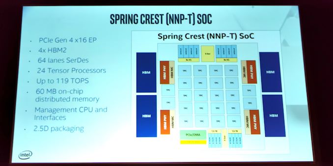
The chip is Intel’s first to support bfloat16 numerics for training in deep learning. Each chip supports up to 119 TOPs, with 60 MB of on-chip memory and 24 dedicated ‘tensor’ processing clusters which have dual 32x32 matrix multiply arrays. The chip has a total of 27 billion transistors, and the cores run at 1.1 GHz. This is supported by 32 GB of HBM2-2400 memory, and technically the PCIe connection is a PCIe 4.0 x16 connection, however Intel does not have CPUs to support this yet.
We were told that for this sort of compute, in order to drive it all, some training customers are moving up from 2P per head node up to 4P, and bigger installations such as Facebook are already using 8P systems to drive their deep learning and training hardware.
Supermicro states that their NNP-T systems are ready for deployment.




15 Comments
View All Comments
abufrejoval - Wednesday, December 4, 2019 - link
With Via's Centaur and the Nervana on a 'last generation node' I wonder if it's time to talk about a 'More's rebound'... It almost seems like a common perception that die shrinks aren't paying off any more.Dragonstongue - Wednesday, December 4, 2019 - link
Moore's actually if this what you are referencing, unless is "play on words" as in, wow those are stonking large GPU sized objects.. as they certainly are that, though to the first one, no, not really as the "law" has morphed many times over the years, in regards to transistor count doubling once every X time frame where now it is "easy" as they can just go MCM (or chiplet) so in effect are still "able" to be on the same cadence.I imagine once they start in the optical interconnect and/or Quantum style, these will likely be very very small jumps in comparison to what becomes the "very first" initial release of..not that you asked, from my reading here and there, they can "easily" go back to the 100s of nm size (as in microns, not nano meters)
as they (optical and/or quantum) not neccersarily play by the same "base rules" are the current silicon based chips / substrate, so they get to start "all over again" which if they were smart, they would do and likely will do exactly this, why start at the very top of the ladder with no real place to go, when you can scale up over many years if not decades as they have done "in the past" which they still pretty much are (though that road is likely to be coming to an end quite soon enough)
(^.^)
abufrejoval - Thursday, December 5, 2019 - link
You caught me snitching an "o" from Gordon, most likely I was named after Sir Thomas More, the lord chancellor of Henry VIII..But it looks like others were surprised by the 16nm TMSC fabbing, too:
https://www.servethehome.com/intel-nervana-nnp-l-1...
Wouldn't it be nice, if one could get the full story on that.
Among my theories are:
1. Intel Fab issues vs. Facebook wanting a product at guaranteed deadlines
2. Power consumption is a much bigger issue at inference because of its scale
3. With the amount of scale-out required to train larger and larger networks, the chip designs become pad bound for all those SerDes anyway, at least until you have truly energy efficient optical links
edzieba - Thursday, December 5, 2019 - link
"It almost seems like a common perception that die shrinks aren't paying off any more. "That's been the case for many years now, generally since 22nm (where gate oxide thickness hit the 1.3nm limit and prevented further transistor scaling, and where 'Xnm' process naming diverged from any real relation to feature size, and beyond which finFETs became necessary).
Process shrinks have produced worse cost/transistor, worse cost/area, and lower maximum operating frequency. The only gains are in transistors/area and perf/watt, so there are only certain applications where it makes sense to move to a newer process: if you are already at the reticle limit and need to go bigger on a single die, or where performance is secondary to power consumption or you are otherwise limited by absolute power output more than operating frequency (i.e. thermally limited). And this scaling is only going to get worse as processes move to EUV and cost/transistor rises even more sharply. This is couple dwith the practical frequency cap introduced by the minimum gate oxide thickness (whey everyone has moved to scaling by adding more cores instead) meaning you need to add yet more transistors.
p1esk - Wednesday, December 4, 2019 - link
Do you know anything about prices or actual performance of these cards?Dragonstongue - Wednesday, December 4, 2019 - link
likely not be at all low cost, as they reference Supermicro and "custom" more or less.also AI Tensor cores and Tbps speed bi-directional links.
I imagine would be / likely will be very fast (for the custom work they need them for)
likely in the many K per unit, all told 2P size (or more) guessing here, in the 20s of K $$ (not to mention custom everything else as well)
wonder their overall power consumption per "rack" and/or cooling required to keep "@ spec"
p1esk - Wednesday, December 4, 2019 - link
They gotta be significantly cheaper and/or faster than equivalent supermicro servers with V100.colonelclaw - Thursday, December 5, 2019 - link
One thing I do know about Supermicro kit, having ordered and built a whole load of it myself, is that it's normally significantly cheaper than the opposition. E.g. our current server cost us £12k as opposed to £20k for the exact same spec from Dell.brucethemoose - Wednesday, December 4, 2019 - link
What Intel needs is a dedicated single socket CPU platform with a boatload of PCIe lanes (128? 192? 256?) and 8+ memory channels, as AI workloads don't necessarily need much CPU grunt.I bet those 4P and 8P setups in particular have mostly idle cores, while the memory controllers are burning tons of power moving and syncing data between nodes.
Santoval - Thursday, December 5, 2019 - link
"This is supported by 32 GB of HBM2-2400 memory, and technically the PCIe connection is a PCIe 4.0 x16 connection, however Intel does not have CPUs to support this yet."Then why mention PCIe 4.0 in their presentation images as a feature? Is this intended to be paired with Intel's current Xeon CPUs or their future Ice Lake Xeon CPUs that will support PCIe 4.0? If it's the former then the images are misleading. It would be like gluing a PCIe 4.0 supporting GPU to a PCIe 3.0 only motherboard and then citing PCIe 4.0 as a feature. A feature that can never be used.